Hi Team
Here are my customer’s issue:
-
In his schematic, there is a step-up voltage about 0.25V which should be 0 V in SDA1,SDA2,SCL1 and SCL2. Could you help me analysis the source of the step-up voltage and recommend me a pull-up resistor value(R115 R116 R117 R118) according to his design and step-up voltage?
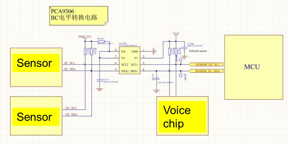

2. There is also a 1V Spike voltage in every 0 status lasting 0.15us in SDA1 and SDA2 happening everytime the SDA changes from 0 to 0.25V. But the whole system is still working normally and the I2C data could be read and written normally ,Could you help analysis the source of the Spike voltage and how to solve these?


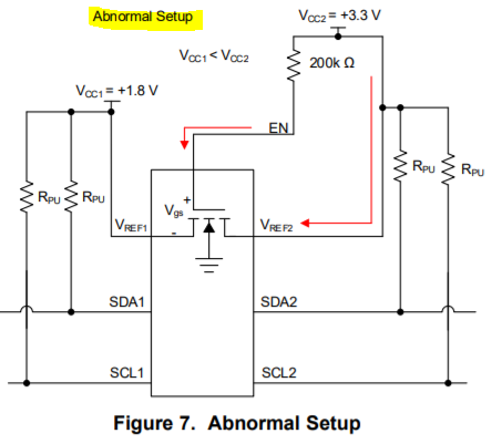
3. In his new schematic, he connect the enable PIN to 1.8V, but he know that this connection is not recommended according in the datasheet, so he want to know what negative consequence could happen if he has to make this change?
Best Regards,
Wesley Huang
Field Application Engineer,China
Texas Instruments Semiconductor Technologies (Shanghai) Co., Ltd
Cell : +86-189-2449-8998
Email: wesley-huang@ti.com