This thread has been locked.

If you have a related question, please click the "Ask a related question" button in the top right corner. The newly created question will be automatically linked to this question.

sn65lvds348 glitch

Other Parts Discussed in Thread: SN65LVDS348

Hi,


we are using the sn65lvds348 quad receiver as an LVDS to LVTTL interface.

The EN control pin is pulled up to 4k7. All the output pins (LVTTL side) are pulled down to GND through 4K7 to ensure a known stat when EN/ is inactive.

EN/ is controlled by a remote processor.

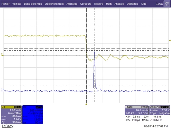
We noticed the following: when the differential inputs are biased such that the output should be a logic zero and the EN/ control input toggles from high to low, a glitch appears at the output 9 ns after EN/ was asserted low.

The glitch size grows when the temperature drops: a glitch of less than 500 mV at ambient becomes higher than 2V at -40 °C.

Is this a known issue? Is there a workaround?

Thank your for your help.

  • Hi, Nicolas,

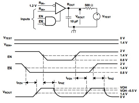
    That's really strange. Could you please post some test waveform just looks like as below, maybe you should monitor some signals: V+,V-, EN, EN/, VOUT at the same time. Then we can help to analyze what wrong with this problem.Thank you very much.


  • Hi Eric,

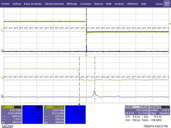
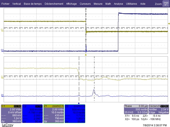
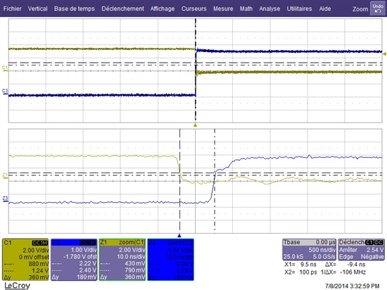
    please find attached 5 scope captures showing the phenomenon. For all 5 captures, the yellow trace is the EN/ control input (pin 9) and the blue trace is the Rout output pin 11. The EN input (pin 16) is pulled-up to 3.3V through 4k7.

    For capture #1, Vrin+ was set to gnd and Vrin- was set to 1.8V => we can see the glitch

    For capture #2, Vrin+ and Vrin- were left floating => there is also a glitch, when the fail safe feature activates, the signal goes high

    For capture #3, Vrin+ was set to 1.8V and Vrin- was set to gnd => the signal goes high directly, no glitch observed

    For capture #4 (ambiant), Vrin+ was set to gnd and Vrin- was set to 1.8V => we can see the glitch

    Capture #5 was performed in the same conditions than #4 except the device was cold

    We monitored the power supply (3.3V), nothing abnormal was observed, it was clean.

    The device is properly bypassed using ceramic capacitors (100 nF + 22 nF), large and short traces.

    Please advise if you need more information.

    Capture #1:

    Capture #2:

    Capture #3:

    Capture #4:

    Capture #5:

  • Hi, Nicolas,

    Thank you for your testing. I am checking this problems with our design team and application team. And we would reply you as soon as possible.

  • Hi Eric,

    I just wanted to let you know that we did additionnal tests:

    we tried to use the EN control pin instead EN/ => no difference, there is still a glitch

    we tried to replace the pull-down by a pull-up resistor at Rout level and set Rin+ > Rin-. In such conditions, when we toggle EN/ from high to low, a glitch also appears(high-low-high) at Rout on some devices we have (not all). And still, the glitch gets bigger when temperature is low.

    we checked all this on different PCB designs (but with the same schematic) => no difference, the layout does not seem to play a role

    we are out of ideas, I wonder if it could be a propagation delay issue inside the chip?  Have you got some news from the design team? Were you able to re-do our tests and observe the same behavior?

    Thanks for your help.

    Nicolas

  • Hi, Nicolas,

    Sorry for replying you so late for I got one week personal training last week.

    I have set up the test as you did, and found the same problem with you.

    Now I am working with our apps and designers to figure out this problem, and I would reply you as soon as possible if we have any  update.

    Sorry again for my delay.