This thread has been locked.

If you have a related question, please click the "Ask a related question" button in the top right corner. The newly created question will be automatically linked to this question.

DS80PCI402 bringup

Other Parts Discussed in Thread: DS80PCI402

Hi,

With the DS80PCI402 PCI repeater/redriver chip. we have developed a board. The above schematics are the control signals of the chip. I want to bring up the board in ENSMB=0 mode(Pin control mode).

We did not use 3 modes(0,1,R,float) instead we skipped R mode. could you suggest me any initial settings through pincontrol mode to be given to EQA0,EQA1,EQB0,EQB1,DEMA0,DEMA1,DEMB0 & DEMB1 to make our board work. to detect the target board.

  • Hi Teja,

    Could you post the schematic again? I am unable to view the graphic. If you have a high resolution pdf that you could attach, that would be even better.

    It is difficult for us to provide a set of good EQx[1:0] and DEMx[1:0] settings without knowing a few additional details about the system. Is it possible to describe the media and amount of attentuation loss (in dB) that you expect to resolve on either side of the repeater? If you could provide a block diagram, that will be helpful. Understanding the amount of trace loss (or cable loss) on either side of the repeater will allow us to recommend a good set of initial settings that you can use.

    Thanks,

    Michael

  • 4152.PCIE_Repeater_Final.pdf

    Hi Michael,


    Thank you very much for your quick reply.

    I have attached the schematics pdf. if you still could not be able to view it. please send me any mail ID to which i will mail the attachment.

    As per the additional details which you have asked, at this point of time even i'm looking to any inputs to understand the requirement. We are using Molex PCIe cable(p/n: 74546-0402), AMPHENOL 9pairs, 5 singles AWG style cable.

    On one side of the repater it is connected in the PCIe slot of a CPU and other side it is connected to a backplane board with a PCI based SATA card. My intention is to see the SATA card in the CPU.

    Could you please give me some pointer to find any information on finding the info about knowing the attenuation loss, euqalization, de-emphasis concepts to understand it better.

  • Hi Teja,

    Please see an intro document we released to provide an introduction about attenuation loss, EQ, and de-emphasis:

    http://www.ti.com/lit/an/snla212/snla212.pdf

    There is also an introduction by Keysight Technologies (formerly Agilent) to describe various types of equipment that are used to provide various test signal condition cases. Please see the link below:

    http://www.keysight.com/upload/cmc_upload/All/2Emphasis-Equalization-Embedding-High-Speed-Digital-Signal-Integrityx.pdf?&cc=US&lc=eng

    For PCIe applications, it depends on which Gen you plan to support. For general-purpose PCIe applications, we recommend leaving RXDET = F, RATE = F and SD_TH = F (auto RX detect, auto rate detect, and auto idle detect). As for the EQx[1:0] and DEMx[1:0] settings, the EQx pin setting is mainly dependent on the amount of loss incoming to the RX of the repeater. The DEMx[1:0] pin setting is mainly dependent on the amount of loss anticipated after the outgoing TX of the repeater. For a good starting point, please refer to p. 13-14 depending on the amount of loss you anticipate on either side of the repeater.

    Some comments on the schematic:

    1. From the schematic you provided, please ensure that on each channel's input and output, there is an AC coupling cap. I see that for pins 28-35 and pins 1-8 that there are AC caps. However, I am unable to tell if there are AC coupling caps on the other side of the connector, so please double-check this.

    2. For 3.3V mode, VDD_SEL should be pulled to GND. I see a DNP on Pin 25 in the schematic. Likewise, for power, please populate 10uF and 1uF decoupling caps (C122, C123). On the VDD pins, 3.3V should never be connected (please remove the potential connection through R20). You may populate R19 if you decide to operate in 2.5V mode, but otherwise, there should be no more than 0.5uF on the 5 VDD pins.

    3. The schematic shows ENSMB = F. This means Master Mode, where all the settings are programmed via external EEPROM. I see an external EEPROM available on J8. Is this correct? If this is the case, then you will not be in pin mode, and you will be relying on what the EEPROM has programmed. Also, if you are in Master Mode, then all EQ and DEM settings will be programmed instead of controlled by pin-strap.

    4. PRSNT# pin should be pulled to GND (normal operation) or VDD (low power mode). Right now it is floating. Typically this pin is tied to an active low PRSNT# signal that is provided by the endpoint device as an analog way to signal to the repeater whether an endpoint is present or removed.

    Hope this helps get you started!

    Regards,

    Michael

  • Hi Michael,


    I couldn't access keysight technologies link.

    in your second point i did not understood the highlighted part. could you please explain in detail

    2. For 3.3V mode, VDD_SEL should be pulled to GND. I see a DNP on Pin 25 in the schematic. Likewise, for power, please populate 10uF and 1uF decoupling caps (C122, C123). On the VDD pins, 3.3V should never be connected (please remove the potential connection through R20). You may populate R19 if you decide to operate in 2.5V mode, but otherwise, there should be no more than 0.5uF on the 5 VDD pins.

    what is problem in using 3.3v or what will happen if i connect 3.3v to vdd
     ?


  • Hi Teja,

    Sorry that the link did not work. I have attached the pdf here:

    4846.2Emphasis-Equalization-Embedding-High-Speed-Digital-Signal-Integrityx.pdf

    For the question about VDD, please see the absolute maximum table and the power supply design requirements from the DS80PCI402 datasheet:

    Regardless of whether you choose to operate in 2.5V mode or 3.3V mode, VDD will be 2.5V. The difference is whether the 2.5V is supplied externally (2.5V mode) or internally via LDO regulator (3.3V mode). 

    If you connect 3.3V to the VDD pins, this may cause damage to the VDD pins due to different power sources applied to the same pins. in addition, applying 3.3V to the VDD pins is beyond the absolute maximum for VDD.

    Thanks,

    Michael

  • Hi Michael,

    These are the settings which i am using in the schematics which i have sent you. could you please correct me if i am doing any mistake.

    1. R19 - 0 ohm to connect 2.5v to vdd (open R20)

    2. R48 - 0 ohm to connect 2.5v to DEMA1 to give supply

    3. R33 - 1K ohm connected to ground DEMA1

    4. R34 - 1K ohm connected to ground DEMA0

    5. C124 - 10uF

    6. C125 - 1uF

    7. R151 - 1k connected to ground -  making LPBK 0

    8. R142 - 1k connected to ground - making ENSMB 0

    RXDET , RATE & SD_TH left float(removed R38,R31 to make SD_TH float)

    9. R40 & R41 - 0 ohm to make the Repeater_PRSNT connect to both the connectors

    10. R46 - 1k ohm to connect it to ground to make Repeater_PRSNT# low as it is active low

  • 1715.pcierepeater.rar

    Hi Michael,

    We are using a molex connector to bridge the Host and target PCIe repeater boards.

    From the above attachment you can understand what i am using.

    First we purchased a OSS PCIe x4 Gen 2 setup. Given below is the link of it.

    http://www.onestopsystems.com/pcie_over_cable_3500.php

    The backplane board which was there in the above attachment i have sent, is taken from OSS and we are using it

    in our Bring-up activity. Will there be any incompatibility issue if i use that backplane board from OSS to our custom developed board

  • Hi Teja,

    Please see comments to your numbered list below:

    1. It really depends on whether you are running in 3.3V mode or 2.5V mode. If you plan to use 3.3V mode, you will need to connect R21 to GND and leave R19 and R20 disconnected (because 2.5V is provided to the chip via internal regulator. You will also need to populate C122 and C123. No external 2.5V supply needs to be applied to VDD if in 3.3V mode.

    If you use 2.5V mode, then you will need to remove R22 and then populate C124 and C125. In this case, connecting R20 is fine.

    2. This is fine.

    3. This is fine.

    4. This is fine.

    5. This is fine when in 2.5V mode. See (1).

    6. This is fine when in 2.5V mode. See (1).

    7. Are you planning to use loopback to root-complex? This means that all B-channel inputs will be ignored and B-channel outputs will provide what the A-channel inputs are seeing. This is not normal operation.

    8. Pin Mode ok. RXDET, RATE, and SD_TH left open ok.

    9.  This is fine.

    10. This is fine.

    I don't foresee any issues with compability for the backplane you are using, as it is created for PCIe Gen-2 and does not have any active elements on it. 

    Thanks,

    Michael

  • Michael,

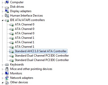
    Attached are the screenshots of the SATA PCIe card detection, using OSS(one stop systems) PCIe repater setup

    in which SATA controller is detected

    .

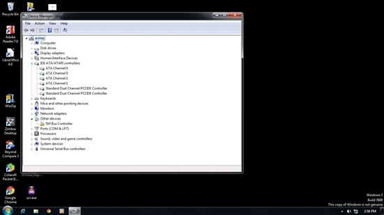
    With our custom board SATA AHCI controller detection did not happen, screenshot is given below

    With our custom board settings, there is no detection. is there anything which i miss. I mean we have done the settings properly, but then too we face an issue in the detection. what am i doing wrong or what am i missing...

  • Hi Teja,

    You may need to explore different EQ and DEM settings to get the controller drive to appear. If you estimate the amount of attenuation loss before and after the repeater, you can configure the repeater so that it provides the appropriate boost/de-emphasis values. It is possible that there is not enough EQ or DEM from the repeater in order for the end system to detect the drive, especially if you have lossy cables on either side. In the past, I have seen detection failure occur on one of our SATA evaluation boards (DS64BR401EVK) due to improper EQ and DEM settings for the amount of cable loss we had on either side of the repeater.

    Thanks,

    Michael