This thread has been locked.

If you have a related question, please click the "Ask a related question" button in the top right corner. The newly created question will be automatically linked to this question.

DS90C387 data mapping question

Other Parts Discussed in Thread: DS90C387, DS90C185

Dear Sir

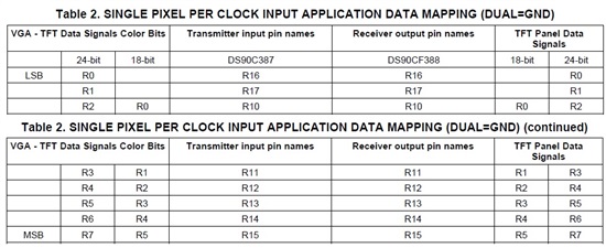
My client have a question about DS90C387 data mapping. They use 24 bit panel. In the datasheet data mapping as below picture.

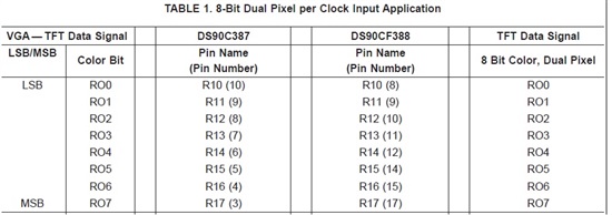
But in the application note AN1162, data mapping as below picture.

DS90C387 data mapping sequence are different in two documents. My customer want to know which one is correct. They are very confused right now.

Thanks

  • James

    I am confused by the reference to AN-1162 - are you referencing: http://www.ti.com/lit/an/snoa089/snoa089.pdf?

    Mark

  • Hi James,

    I was unable to locate AN-1162 (as Mark mentioned, it seems to be an app note about the LMX3162?). However, I think I may be able to comment on this confusion. There are several ways to map the VGA-TFT color bits. Please see the LVDS output mapping for 24-bpp (assume single pixel, so only 4 LVDS pairs):

    There are several practices for how to approach situations where you need operation with 18-bit or 24-bit. Typically, customers will either place the 2 LSBs in LVDS pair A3, or they will place the 2 MSBs in LVDS pair A3. In the DS90C387 datasheet, the convention is to place the 2 LSBs so that they are mapped to A3. That way, if you choose to operate at 18-bpp, you will still get the highest resolution available with pairs A0-A2, while A3 can be disconnected. The app note you are referring to appears to be doing the other acceptable practice, where the 2 MSBs are mapped to A3. 

    To ensure compatible mapping, please look at the mapping your deserializer/TCON requires. As long as you know which pin the specific RGB bit will appear on the deserializer, you can choose either conventions. I recommend using the mapping in the DS90C387 datasheet for simplicity.

    An especially helpful document to understand these conventions further is the DS90C185 datasheet. On p. 11-13, you can observe the way that you can place MSBs or LSBs on CH3 (or LVDS pair A3).

    Thanks,

    Michael

  • Hi Michael

    After checked the application note is AN1163. I'm sorry for wrong input.

    Would you please help check AN1163 and DS90C387 datasheet data mapping which one is correct.

    Thanks

    James

  • Hi James,

    Either is acceptable, depending on how you want to organize the highest LVDS pair. Please see my previous explanation in my last post.

    Thanks,

    Michael