This thread has been locked.

If you have a related question, please click the "Ask a related question" button in the top right corner. The newly created question will be automatically linked to this question.

DS15EA101: LOS and EN Pin Timing

Part Number: DS15EA101
Other Parts Discussed in Thread: DS90LV001

By the way, does anyone know what exactly EN pin does?

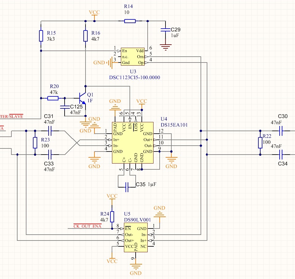
Have 2 lvds clocks electrically paralleled (=wire or'ed), one from a DSC1123 100MHz mems oscillator, and the other from an incoming diff pair.

The latter gets equalized by this DS15EA101, when available and selected.

For selection, I do manage the EN pins for these two devices in order to change the source available on common output lines.

The strange i see is a low frequency on/off pattern superimposed on the 100Mhz clock. It varies in frequency as i do probe or touch the equalizer external capacitor at pins 5&6.

But EN is low!  should'nt it disable the outputs, hence any influence of the ds15101 on it's outputs?

And, will the 50 ohm internall pull-up terminators stay there also when disabled?

Thanks for your help!

Francesco

  • Hi Francesco,

    EN pin is true on low and it enables the output. In other words, this is output enable - true on low. When this pin is low output is enabled.

    When disabled, the output is muted and it has a constant level - constant high or low.

    Could you please let me know what is your application and are you AC coupling to the output of the DS15EA101? If possible please send me a block diagram of your application.

    Regards,,,nasser
  •  Hi and thank you for the reply. I had discovered myself about polarity later after posting this request.  (discard the bjt, already removed on my prototype board)

    Anyway, i still have a problem: As you can see, when i designed it i was persuaded i could disable one of the DS1123 or the DS15EA101 and have the bus fully in control of the enabled one... But as far as i can scope out the LVDS swing is deeply reduced by the disabled DS15EA101 outputs, and furthermore this reduction is much higher for the negative output w. respect to the positive one... . And albeit the following receiver seems able to recover the clock, i'm not shure it won't jitter more than expected

    F.

  • Hi Francesco,

    When DS15EA101 is disabled, it still provides 100-ohm termination on it's output. A combination of DS15EA101 and R22 100-ohm terminations provides double termination. Maybe you can increase R22 to about 130 ohm and this will reduce signal attenuation that you are seeing.

    Regards,,,nasser
  • Thanx.

    i guess a 6dB attenuation should not be a problem: the cable will be short, the frequency not that high (100Mhz).

    What really disappoints me is that this reduction is much higher for the negative output w. respect to the positive one.

    It behaves like if:

    1) the output gets not disabled, but halted in a certain logical 1 state (outp=1, outn=0)

    2) the impedance presented on the output is not constant but drops to a much lower value when in low state

    condition  1)  was confirmed by the datasheet, that i had not read as carefully as i should have done before designing.

    condition 2) is more hard for me to understand, for at least a couple of reasons.

    As far as i know, LVDS should be based on a current steering concept. A current generator gets steered from one of the legs to the other or viceversa, every time inverting the voltage difference presented on outputs.

    If that's true, the impedance seen on output pair should be constant, right? (a current source has high impedance) . So why do i see the output loading much more it's line when low, than when high?

    The second reason is that if real, this impedance shift would vanify every attempt to terminate the bus:  when terminated with the right load for the 0-1 transition, it would not be the same for the 1-0 transition... this can't be.

    There must be something else, probably due to the fact that different LVDS chips are compatible, but not identical for output structure and output common mode voltage range. So a low level forcing too low the line compresses the available swing for the other driving device to a small range just over the gnd rail, while the high on the other, releasing the current source, leaves the whole room to it's companion driver.

    This all just for helping others using this equalizer profitably. For what concerns my design, have decided to change the DS15EA101 for a simple DS90LV001,  it doesn't equalize but is enough sensitive to recover a somehow attenuated input, and has a true output enable/disable (rather than a signal-chain enable/disable) control pin.

    Francesco