This thread has been locked.

If you have a related question, please click the "Ask a related question" button in the top right corner. The newly created question will be automatically linked to this question.

TCA9406: Why is gate bias set at approximately the VCC level of low voltage side plus one threshold voltage?

Part Number: TCA9406
Other Parts Discussed in Thread: PCA9306,

Hi there supporter,

I am checking the working principle of NMOS transmission gate and I am wondering the reason why is gate bias set at approximately the VCC level of low voltage side plus one threshold voltage.

Can you let me know that?

Regards,

S.P. Lin

  • Hello S.P. Lin,

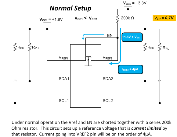
    This is how the part is designed to work.  In order to turn on and off the pass fets we need to setup a reference point to the internal pass fets.  I have attached a simplified diagram of the PCA9306 which shows how that is setup. 

    Once you have the bias, then you can setup how to turn off/on pass FETs.  The TCA9406 than add national features such as internal pull ups and Rise Time Accelerators, but the basic premise of how to setup a reference for the pass fets is the same.  Is this clear enough for you?  Why are you asking about this so I can understand the question better.

    -Francis Houde

  • Hi Francis,

    I am trying to explain to my staff that why TCA9406 cannot be used as a repeater and what I am going to say is based upon the capacitance. Since the current flow will go through both two sides when TCA9406 is conducting, all the capacitance on both side should be taken in to account. And compared to the buffered I/O, always the input resistance is close to a very large number, therefore the current flow goes in to the buffered translator can be considered as approximately to zero. As a result, only single side's capacitance should be accounted and that is why we call it as a "repeater". However, when I was talking about TCA9406's switch structure, I had no idea about the gate bias.

    Additionally, based upon the screenshot you provided, I still cannot really understand why the gate voltage of the PMOS passgate will be the lower side voltage plus a threshold voltage. Can you explain it in detail for me?

    Your kindly help will be appreciated.

    Regards,
    S.P. Lin
  • Hi Francis,

    Actually, I thought the passgate type for the gate bias should be NMOS instead of PMOS. And having NMOS's gate and drain tied together makes it always works in saturation mode. Thus, the NMOS passgate is turned-on and gate (or drain) voltage is continuously discharging until the voltage of gate (or drain) drops to voltage of source plus a threshold voltage. Please let me know if anything wrong. Thanks a lot.

    Regards,
    S.P. Lin
  • Hello S.P. Lin,
    So your explanation about the why the TCA9406 can't be used as a buffer is correct. I also didn't realize that I had not configured the fet correctly in the drawing. I have changed it now. It is a N-FET with the body isolated. Sorry for the confusion.
    -Francis Houde