This thread has been locked.

If you have a related question, please click the "Ask a related question" button in the top right corner. The newly created question will be automatically linked to this question.

TCA8418: the tca8418 for gpio mode

Part Number: TCA8418

In the datasheet,8.6.2.8 GPIO Data Status Registers, GPIO_DAT_STAT1–3 (Address 0x14–0x16),there is "These registers show the GPIO state when read for inputs and outputs. Read these twice to clear them".Does that mean that I can not read the gpio state more than twice?and now I did these following in linux。

1.

error = tca8418_write_byte(chip,REG_KP_GPIO1,0);
error = tca8418_write_byte(chip,REG_KP_GPIO2,0);
error = tca8418_write_byte(chip,REG_KP_GPIO3,0);

2.

error = tca8418_write_byte(chip,REG_GPIO_DIR1,0);
error = tca8418_write_byte(chip,REG_GPIO_DIR2,0);
error = tca8418_write_byte(chip,REG_GPIO_DIR3,0);

And then,when I read the reg ‘GPIO_DAT_STAT1’,I always get a constant number,like 0xbf,even if  i changed the gpio level through 3.3V or GND with a 10k resistance.

so,anyone can tell me,when I want use tca8418 only in gpiomode,how should i init it, and get or set the gpio's value.

  • Hello,

    The errors you are seeing I believe is issues with code. Unfortunately our team does not support the software side of the devices so I won't be able to provide you with much on that end. Though it looks like you are able to get ACKs because you can read. Maybe the address is wrong for your write function?

    "Does that mean that I can not read the gpio state more than twice?"
    -You should still be able to read the gpio state but it will likely clear after two reads.

    Note, the "REG_GPIO_DIR" registers are default 0 or inputs so you do not need to write to these.

    "And then,when I read the reg ‘GPIO_DAT_STAT1’,I always get a constant number,like 0xbf,even if i changed the gpio level through 3.3V or GND with a 10k resistance."
    -I believe the numbers here are latched because the "REG_KP_GPIO" registers are in keypad mode and need to be in GPIO mode. It may also be because the device has internal pull ups enabled on the GPIOs upon start up.

    Can you provide a schematic we can double check?

    Thanks,
    -Bobby
  • I have used an  oscilloscope to get I2C SDA line.

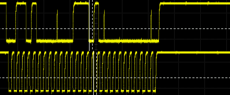
    first I send the commod " tca8418_write_byte(chip,REG_KP_GPIO1,0)"

    and then i can get the  following waveform

    Because my oscilloscope is a single channel,so these two pictures are  syntheticed by me。  

    and Can I prove I2C communication is normal throught the pitcure?

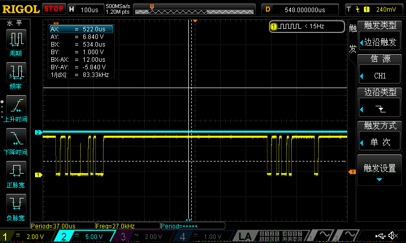
    when I read the register  GPIO_DAT_STAT1,I can get the following waveform:

    and you can see that the slave is not respone at once,and these is also no ACK when I send the register addr to slave。All the read  is different form the datasheet about read register like this

    so could you tell me,why there is no ACK when I read the register.thanks.

  • Hello,

    From the scope shot of SDA/SCL you've shown, I believe I can make out what is being sent and received:

    First message is 0x34h R/W'=Write ACK

    Second part is 0x1Dh ACK

    Third part is 0x00h ACK then release I2C lines.

    From this, it looks like you are successfully able to write to the register because there is an ACK in all three cases. So I don't understand why in software it tells you there is an error.

    ------------------------------------------------------------------------------------------------------------------------------------------------------------------------------------------------------------

    Your second o-scope picture, I can't read the data because the SCL line is not there for reference, I can see that from the old picture ACKs are shown after master released SDA line so there is a small spike. There is only one small spike in the first half of the picture which states the device ACKs for its address but not for the register ID.

    Can we try to confirm read works with a different register like 0x04h or 0x1D after you write to it?

    Thanks,

    -Bobby

  • this is the picture,When I read the register GPIO_DAT_STAT1。

    Is there anything unusual here?

  • It looks like in the first half of the picture you are writing to 0x34h write then 0x14h and you get an ACK for both. However your clock signal hangs low instead of releasing the SCL line. This could be a problem for the state machine so it would be best if you did a stop condition and then did a start condition again to continue trying to do a read.

    The Second half of the signal is a bit hard for me to read but looks like you are sending the address again 0x34h with a read bit and then receiving 0xAF (a bit hard for me to read). I do see that on the last clock cycle, it looks like the master is ACKing but then you do a stop condition which could glitch the state machine because it is expected a NACK and a stop condition instead of an ACK and a stop condition. This may be why you are seeing the GPIO_DAT_STAT1 getting stuck. Are you able to send a NACK instead and then try doing a read again after referencing GND/Vcc (reference all the inputs to GND)?

    -Bobby

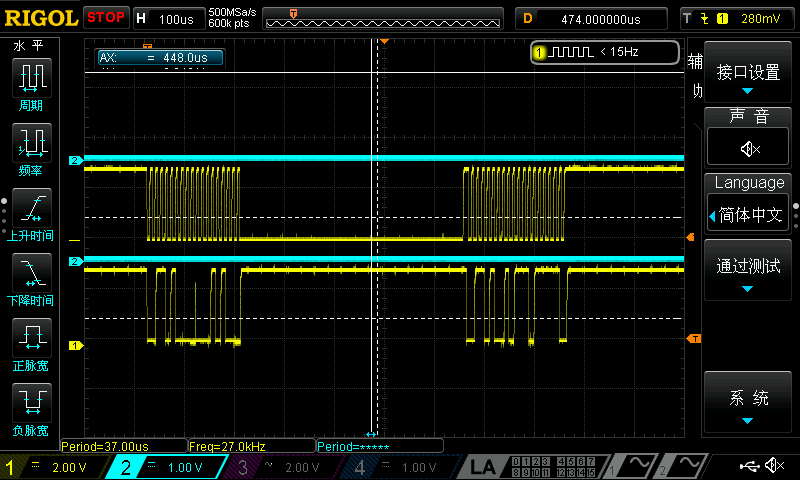
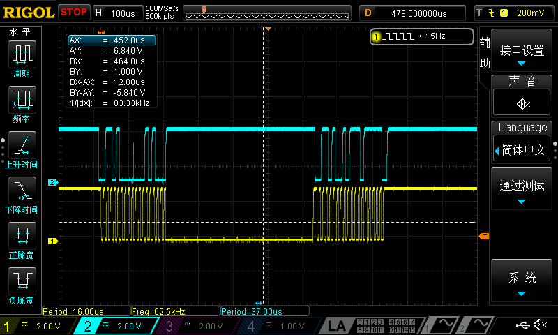
  • Happily,I can finally use the dual channel oscilloscope。And when I read the register GPIO_DAT_STAT1,I can get the picture belowing

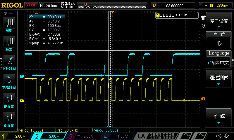
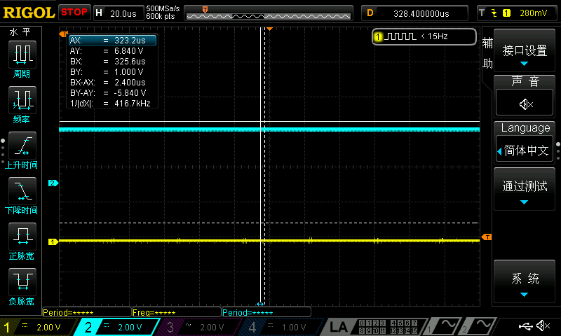
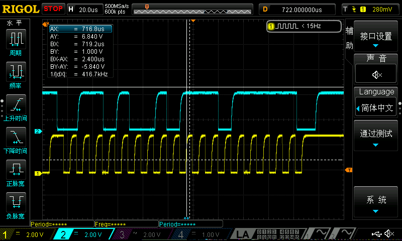
    and then,I  divided the entire waveform into three parts,I divided the entire waveform into three parts and magnified them separately for your observation.

    The first half

    the second half

    and the last half

    please tell me,is there any    int these pictures?

    Or I can refer directly to your last reply?

  • I change the gpio level ,and read the register GPIO_DAT_STATx,it is a right value
  • Hello,

    The new waveforms are much easier for me to read (thank you). It does indeed look like in the last picture when you read, the value is 0xEFh which suggests you are holding Row 4 pin low. Are you not doing this? The new waveform also looks like you are NACKing after you receive the data which is good.

    In the first waveform after the first ACK, there is a small "glitch" where it looks like the slave who ACKs releases the SDA line and then a small amount of time later the master pulls low. It doesn't look like this will cause problems for you though as we sample data in the middle of the high period of the SCL line.

    I see in your last post it looks like you've got the device working the way you intended, did you make any changes to make this work?

    Thanks,

    -Bobby

  • Tanks for your help these days,I make the I2C bus speed to 400khz yesterday,but I think that's probably not the main reason.Maybe at first, I wasn't careful enough with the chips.

    and about read twice to clear it,it iis maybe means read twice the register will be updated by the chip.

  • Hey Haohb,

    Thank you for getting back with us on how you were able to resolve the problem. I've marked your last post as the resolved statement for others to refer to if they have similar issues.

    "and about read twice to clear it,it iis maybe means read twice the register will be updated by the chip."
    This probably means there is likely two Flip-Flops connected to the input meant to monitor when the button was pressed and released.

    Thanks again,
    -Bobby