Other Parts Discussed in Thread: TCA9617B, TMP75
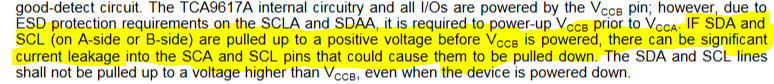
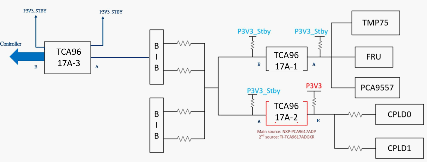
The TCA9617A/B internal circuitry and all I/Os are powered by the VCCBpin.
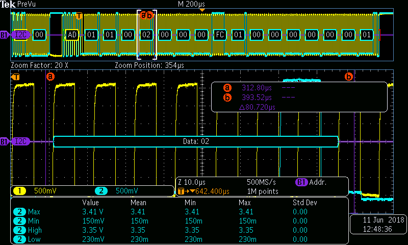
If VCCB pin was not powered, what are the A-side pins (SCLA and SDAA) state? H-impendence in 9617_Channel A internal? Or else?