This thread has been locked.

If you have a related question, please click the "Ask a related question" button in the top right corner. The newly created question will be automatically linked to this question.

Inquiry regarding Short-circuit output current on ISO3080

Other Parts Discussed in Thread: ISO3080

Hello, all

Now we are considering to use ISO3080 for next design model, then would like to know the detail on its Short-circuit output current.

Please see the comment below, and feedback us with your comment.

On page 3, this term is defined as -200mA to 200mA. We understand that this definition is for the case that the RS485 differential line is shorted between + and -, by the means of internal current limit.

Please let us clarify whether this current limit is also applied in case + and GND or - and GND are shorted. 

We thank you in advance for your information.

Best regards,

  • Hi Okui-san,

    This parameter in the datasheet specifically refers to how much current the driver will sink, not source. The idea behind this parameter is to test how much current one driver will sink if multiple drivers in parallel are sourcing current and there is a ground potential difference.

    The RS485 standard limits the amount of current that any driver is able to sink to a maximum of 250mA. This is not a requirement of how much current the driver has to be able to sink, but instead of a maximum amount that it is allowed to. Since the maximum voltage a bus pin is required to withstand by the standard is from -7 to +12 volts, this current is measured at the extremes. One bus pin is held at +12 and -7 volts, while the other is tied to ground and the driver is enabled. Then the opposite is done. In all four conditions the amount of current that the driver sinks is measured. The datasheet parameter depicts the maximum amount of current the driver will sink for any of the four conditions.

    Thanks,

    John

  • Hello Griffith-san,

    Firstly, thank you for your previous support regarding Short-circuit output current on ISO3080.

    Apart from this inquiry, we would like to know the detail of some absolute maximum ratings for VO and VIT.

    Please refer to the items below, and feedback us with your comment.

    On these terms of description, we assume that –9 to 14V for VO and –50 to 50V for VIT are both aimed for the voltage limit which is applied between "A, B, Y and Z" and "GND", not for between A and B or Y and Z.

    Please let us clarify how much voltage could be defined as absolute maximum ratings between A and B or Y and Z.

    We thank you once again for your information.

    Best regards,

  • Okui-san,

    You are correct with your interpretation of the VIT and VO parameters in the datasheet. From the "Recommended Operating Conditions Table" we guarantee that the device can handle ±12 input differential voltage from A to B.

    Unfortunately I do not have any information on the maximum differential voltage between the bus pins, so I will need to check with design or characterization to see what other information that they have. This may take a couple days to get some feedback.

    I will let you know when I hear back.

    John

  • Griffith-san,

    Thank you for your prompt reply on this inquiry.

    Regarding maximum differential voltage on VIT, we are looking forward to hearing from you again.

    Best regards,

  • Okui-san,

    I am waiting for design to verify what I beleive will be the answer, and I have requested some sampes so I can test the devices in the lab to verify what we find. Sorry for the delay in getting the answer to you. I will update you early next week.

    Thanks,

    John

  • Okui-san,

    Design verified that the device will not be damaged if both the bus pins remain within their "Absolute Maximum" ratings.

    The bus will see the same impedance with respect to the A & B pins when the receiver is in both the enabled and disabled states.

    In terms of the driver, or the Y & Z pins, they will be high impedance (<±1µA of leakage current) when the driver is disabled, but will be very low impedance when enabled. This would be my only concern, that when the driver is enabled, and shorted to high voltages within the absolute maximum table, the Y & Z bus pins will sink / source a lot of current. This could result in the device heating up and going into thermal shutdown.

    Thanks,

    John

  • Griffith-san,

    Thank you for your previous support towards the inquiries regarding ISO3080 from our customer.

    I have some additional inquiries regarding insulation characteristics on this device.

    Please refer to the items below, and feedback us with your comment.

    We would appreciate if you could show the detailed test condition of VIORM, VPR, VIOTM and RS individually.

    If you could not show, please let us clarify at least following information.

    VIORM: Between on which pin did you test for this characteristic? and which test condition did you apply for this test?

    VPR: Did you test this between R /RE and A B, and D DE and Z Y?

    VIOTM: Between on which pin did you test for this characteristic? 

    RS: Does TS stand for Maximum case temperature (150 degree)? and between which pin does VIO was tested?

    We thank you once again for your information.

    Best regards,

  • Hi Okui-san,

    Sorry for the delay in getting back to you. The E2E site was under maintenance yesterday afternoon.

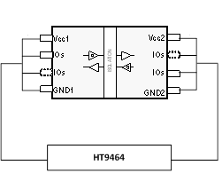
    All of these tests are performed with the pins one side 1 of the devices shorted together and the pins on side two of the device shorted together. Therefore, only the isolation barrier is being tested. See picture below.

    VIORM is the repetitive voltage stress that the isolator can handle over its entire lifetime. It is tested by applying a much higher repetitive voltage to the isolation barrier and measuring the time to failure. After this accelerated lifetime test is done the data points can be used to extrapolated the lifetime of the device at lower voltages.

    You are correct, TS stands for maximum case temperature. This is shown in the table on the bottom of page 10 in the datasheet.

    Please let me know if you have any other questions,

    John

  • Griffith-san,

    Thank you for your reply towards the inquiry regarding ISO3080 from our customer.

    With regard to the test condition of RS, please let us clarify whether this test is also performed with shorted all pins on side one and side two individually or only 2 IO pins on each side.

    Since the datasheet describes VIO = 500 V, then we would like to clarify whether this is also applied for same condition that you mentioned above.

    We thank you once again for your information. 

    Best regards,

  • Hi Okui-san,

    The RS test in the datasheet is measured with the device at 150°C with all the pins on each side of the device shorted together (all pins on side 1 shorted together, and all pins on side 2 shorted together). The resistance between the two sides is then measured with a 500 volts across the isolation barrier. Since all the pins on side 1 and all the pins on side 2 are shorted together the lowest impedance path between the two sides will have the largest effect on the end result.

    Thanks,

    John

  • Griffith-san,

    Thank you for your continuous support towards the inquiries regarding ISO3080 from our customer.

    With regard to the test condition of VPR and VIOTM, we have some additional questions. Please refer to the item below, and feedback us with your comment.

    We understand that the test condition of VPR is t = 1 s then 1050V as a result.

    Meanwhile the test condition of VIOTM is t = 60 s then 4000V as a result.

    Please let us clarify why the VIOTM is higher than higher than VPR, since the test time of VIOTM is longer than VPR. 

    Also, we would appreciate if you could let us know what does "Method b1" stand for.

    We thank you once again for your information.

    Best regards,

  • Hi Okui-san,

    The1 second test is what we do in production, while the 60 second test is what is done at the certified test lab for qualification tests at VDE.

    Method B1 refers to how we test the device in production. This includes the VIOTM test and the VPR test. Method B1 does both tests back to back and method B2 has a delay added between the two.

    Thanks,

    John