This thread has been locked.

If you have a related question, please click the "Ask a related question" button in the top right corner. The newly created question will be automatically linked to this question.

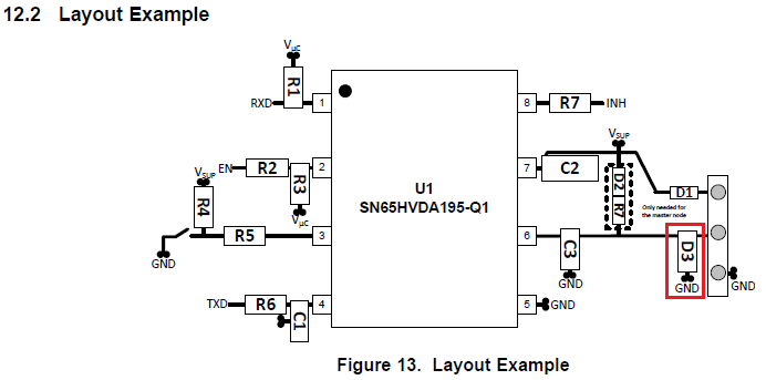
SN65HVDA195-Q1 / Layout Example(Figure 13.)

Guru 29690 points
Other Parts Discussed in Thread: SN65HVDA195-Q1

Hi Team,

Layout Example of SN65HVDA195-Q1 shows the following D3 diode.
Is it zener diode?
I would also like to ask how to select the diode.


Best Regards,
Yaita / Japan disty

  • Yaita-san,

    This is a transient voltage suppression (TVS) diode that can be used if additional transient protection is needed by an application. It should be chosen such that its reverse breakdown voltage is higher than the LIN voltage range (so that the diode leakage current remains small enough to not impact operation), and its peak voltage during a transient is below 40 V (the absolute maximum rating of the LIN pin).

    Regards,
    Max
  • Hi Max-san,

    Thank you for your answer.
    Is there any restriction for capacitance of TVS diode?
    I heard my customer considers to use the value of 30pF.

    Best Regards,
    Yaita

  • Yaita-san,

    Using a high capacitance could limit the maximum data rate that can be achieved on a link. Since the dominant-to-recessive edge is driven through relatively weak pull-up resistances (rather than a low-impedance driver), the signal's transition time is largely dependent on the capacitive loading of the bus. The 30 pF capacitance of the TVS should be low enough to not cause issues, though.

    Best regards,
    Max