This thread has been locked.

If you have a related question, please click the "Ask a related question" button in the top right corner. The newly created question will be automatically linked to this question.

RS485 to replace Max13085

Other Parts Discussed in Thread: SN65LBC182, SN65HVD82

Hello Team, 

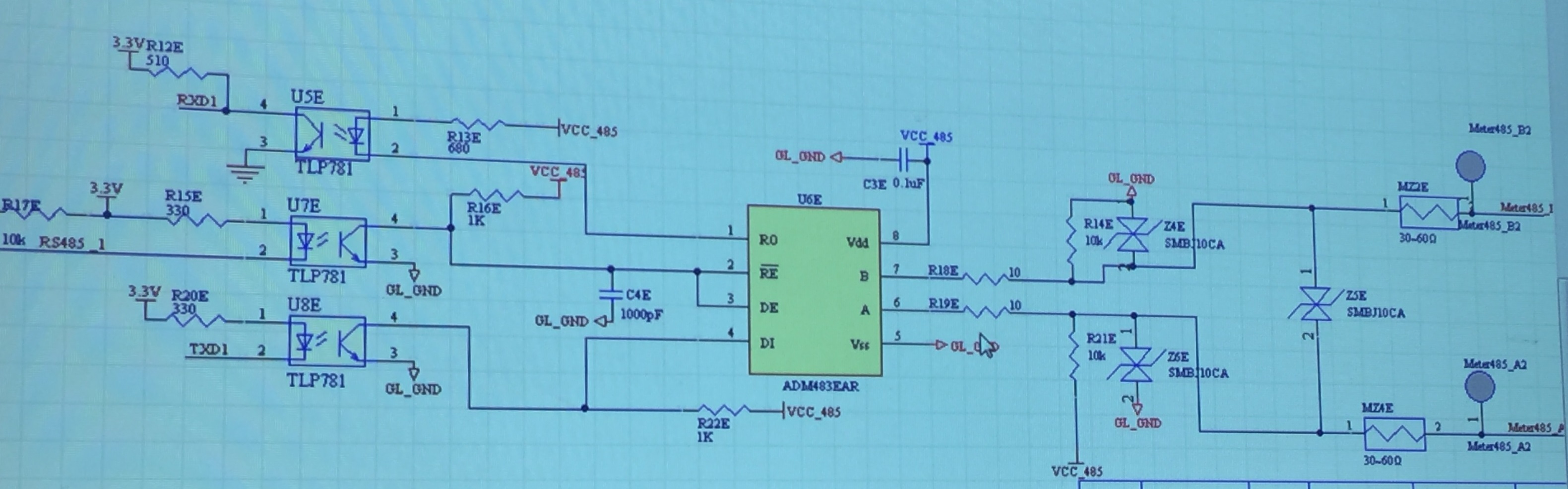
My customer has been using SN65LBC182 in their China southern grid type II concentrater project.

Recently they have reported that out LBC182 has failed to take more then 40 load units on the bus. When the load units on bus are more than 40, LBC182 can pull below 0V.

Do we have any alternative to replace MAX13085 which has large output current?

Below is customer schematic. The pull up and pull down on load unit side is 20k.

Thanks and best regards,

Victor

  • Hi Victor,

    What data rate is needed, and what is the maximum number of nodes that can be supported. Would SN65HVD82 work? It is a 5-V RS-485 transceiver with integrated IEC ESD protection.

    Best regards,
    Max
  • Hi Max,

    Data rate is 2.4kpbs, the maximum number of nodes is 192 and the actual tested number of nodes is 40 to 50. SN65HVD82 result is similar as LBC182.

    The scope capture shows the send and receive signal on the bus.The second capture is the expended of the received signal.

    Below capture shows a normal received signal waveform.

    Best regards,

    Victor

  • Hi Victor,

    Sorry for the delay; I was out of office last week. These waveforms look very strange to me. An RS-485 transceiver is not capable of driving voltages that are outside of its supply range (below ground or above VCC). Can you please tell me which signal is being measured, and how the measurement is set up
    (ground connections, probe/scope impedances, etc.)? Something like a block diagram may be helpful in giving us a better understanding what is going on.

    Best regards,
    Max
  • Hi Max,

    Rechecked with customer. Please refer to below update.

    1. The prob is connected between 485 BUS node A and node B. The power supply 485 is 5V.

    2. Below waveform is tested using 3-wire controlled 485 as master and 2-wire 485 as slaver.


    3. Below waveform is tested using 3-wire controlled 485 as master and 3-wire 485 as slaver.

    2-wire controlled 485 schematic

    3-wire controlled 485 schematic

    Best regards,

    Victor

  • Hi Victor,


    Max asked me to help him work through this with you and I have a few additional questions after reading through the thread.

    1.) In your first post, you mention that the "LBC182 has failed to take more then 40 load units on the bus."  The RS485 standard typically considers 32 Unit Loads as the maximum.  Am I correct in understanding that they are trying to create a bus with enough nodes that would cause the loading to be equivalent to 40 Unit Loads?

    2.)  How many nodes are connected together when the scope images were captured?  You mentioned that only 40-50 nodes were tested.  Were all of them connected at the time the image was taken?

    3.) What type of cable is being used to connect the BUS pins?  And how long are the cable segments between nodes?  Are also they of equal length between each node?

    4.)  Is the same problem observed with fewer nodes connected to the bus?  At how many nodes connected does the problem start to be visible?

    5.) I don't see a decoupling capacitor on the VCC pin in the 2 wire controlled schematic, is this correct?

    The waveform in the scope images you have provided look like they are being affected by a bus with lots of capacitance.  Any additional information you can provide to my questions will help me better understand the bus and help identify the problem and a possible solution.

    Thanks and Regards,

    Jonathan

  • Hi Jonathan,

    Thanks for your help.

    1.) Well, the actual application is that one concentrater will be connected to 40-50 e-meters. Thus I am saying that LBC182 will take more than 40 loads.

    2.) Just one concentrater to one e-meter only.

    3.) it's 1200m twisted-pair wire.

    4.) see 2)

    5.) No, there is on cap on VCC in 2-wire scheme.

    Best regards,
    Victor
  • Hi Victor,

    Thank you for the additional information. I have a few additional follow up questions.

    1.) Am I correct in my understanding that the 3-wire controlled schematic is used in the master node in the concentrater, and the 2 wire controlled schematic is used for all the other 40-50 slave nodes in the e-meters on the BUS?

    2.) During the test, are all devices TI devices, or do some of the nodes contain competitor devices as seen in the two schematics?

    3.) Am I correct in my understanding that if the 3-wired controlled schematic is used in the slave nodes? This would mean that the source of the problem is in the way the 2-wire controlled schematic uses the RS485 transceiver.

    4.) How is the bus terminated and with what value resistors?

    I noticed that the AZRS485 device was used in the 2-wire schematic. I have seen this implementation before related to that brand of transceiver. They are using the RS485 transceiver a little differently than most RS485 transceivers are designed to be used by connecting the D pin to GND with a 1K resistor and enabling/disabling the driver with the data signal. This relies upon the pullup/pulldown biasing resistors to pull the A/B Pins to a differential voltage for a "1" by disabling the Driver, and then actively drives the bus by enabling the Driver which is set to drive a "0" by the 1K pulldown resistor on the D pin.

    This explains why the rising edge of every data bit shows the RC time constant which is a product of the overall effective biasing resistors and bus capacitance. Changing the biasing resistors or lowering the bus capacitance by making the bus shorter and or reducing the number of nodes on the bus will change that RC constant and could improve the shape of the bit. For example, reducing the biasing resistors to 1K would help the rising edge, but with 40-50 nodes on a bus, that would put 40-50 1K resistors in parallel and become to strong of a bias to allow for a the driver to overcome when driving a "0". There is a fundamental difference in the way the AZRS485 handles the DE/RE circuit that is different than most other RS-485 transceivers that allows them to drive the bus in this method.

    If the 3-wire schematic works in the slave nodes, it would be a better option for use with the SN65LBC182. It could be possible to reduce the BOM cost on that method as well by removing a couple of the TVS diodes. It is not common to have 3 of them (2 single ended and 1 differential) in a system at the same time. The differential TVS diode is probably all that is required, and also similar to the 2-wire schematic version. That could help offset the cost of the additional control wire on the D pin.

    Regards,
    Jonathan