This thread has been locked.

If you have a related question, please click the "Ask a related question" button in the top right corner. The newly created question will be automatically linked to this question.

SN65HVD33

Other Parts Discussed in Thread: SN65HVD33

When using SN65HVD33 devices for a 4 Mbps half-duplex connection with ~4m meters of cable, 120 ohm termination at each end, we experience following behavior:

The first bit in at transmission after a bus idle is corrupted by the driver it seems that the driver has a delay from DE=1 to Y,Z valid of ~400 ns when the bus has been idle for milliseconds. However if the idle period was less (like <100 us) DE=1 to Y,Z valid is <30 ns.

Please see below (D is channel 4, Y is channel 3, Z is channel 1, DE shifts from 0 to 1 at the dashed cursor)

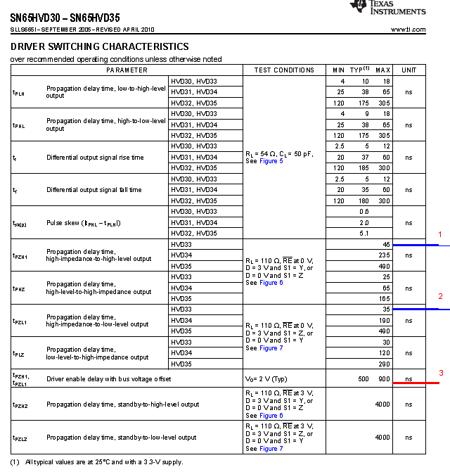
A DE=1 to Y,Z valid =~ 30 ns matches to the datasheet (SLLS665I –SEPTEMBER 2005–REVISED APRIL 2010) page 6, marks 1 and 2

Whereas the ~400 ns maybe matches the mark 3 spec.

Questions:

Is it correct that a long bus idle time (> 100 uS) will provoking a long tPZH1/tPZL1 of more than 400 ns?

1 If yes, why and how do we avoid it?

2 If not, what is then the cause?

- Could you please explain the spec. Driver enable delay with bus voltage offset

  • In our design DE and REn are tied together and driven by the UARTs Transmit Enable – so I don’t see how we can end up in Low power standby mode

    We have also tried to tie REn to Gnd and only drive DE with the UARTs Transmit Enable, with same result.

  • Andy,

    sometime when a common-mode voltage close to Vcc or a non-balanced code (with DC content) charges up the capacitance of the bus lines then long delays of Vod can occur after long idle times. the reason for that is the gate capacitance of the large output FETs of a driver's output stage. during transmission the bus is driven by a driver and therefore low-impedance. A driver's gate capacitance are charged and discharge fairly quickly. During idle time, the bus becomes high-impedance. At this time the same gate capacitance are charged reversely to avoid leackage current flowing back into the driver out put. The higher the bus voltage the higher the reverse gate charge. Then, when transmission starts again, the large gate charges have to be discharged and charge in the opposite direction. The higher these charges were, the longer the discharge times and the longer the response time of the driver to assume the correct Vod.

    Suggestions:

    1) make sure that any common-mode does not exceed the Vcc

    2) the use of external failsafe resistors keeps the bus lines at a certain potential

    3) the use of balanced code avoids charge up bus capacitance.

    Hope that helps.

    Best regards,

    Thomas


  • Hi All,

    We are seeing a similar issue.  I know it is a long shot, but any chance you know how this issue was resolved? 

    For the resistor solution, can you provide guidance on the sizing of the failsafe resistors? Do these go across the line (Y to Z)?

    To add to our confusion, the datasheet shows that the device has 5V tolerant inputs on the logic side and the recommended operating conditions suggest that the device can withstand -7 to +12V of common mode.

    We have seen the device start to drive and then gives up creating a runt signal.  Our system may to be triggering an internal fault that is being acted upon by the chips internal circuitry, but still odd.

    Also, we use biphase differential encoding on these lines which means that the average DC bus value is 0.

    Any help would be appreciated.

    Thank you

  • Hello,

    Given the age of this thread, I can't say how the above was ultimately resolved.  To best address your issue, I would ask that you start a new thread, and share a schematic and scope shots (D input, Bus differential, R output, etc...)

    To address your specific questions, 1) Failsafe resistors are placed between the A line and VCC, and between the B line and ground to establish a known, positive DC voltage on the bus when it is idle (no active drivers).  See this application note for specific procedures on choosing failsafe resistor values, and how they can affect bus loading.

    2) The -7V to +12V common-mode range refers to the bus pins, A and B. Per the Recommended Operating Conditions, these terminals should remain between -7V and +12V.

    The statement about 5V tolerant inputs refers to the logic inputs (D, DE, RE).  That is, when VCC = 3.3V, you may still use 5V logic signals to control the D, DE, and RE inputs.  Unlike the bus inputs, the logic inputs should remain between 0V and 5V.