This thread has been locked.

If you have a related question, please click the "Ask a related question" button in the top right corner. The newly created question will be automatically linked to this question.

UCC21520: Please tell me about the operation of UCC21520.

Part Number: UCC21520
Other Parts Discussed in Thread: TINA-TI

Hi, team.

My customers have started designing circuits using UCC 21520.

Although the operation is confirmed using the SPICE model of this device,

It is not an intended action.

Can you tell me whether this behavior happens even with real devices?

※ The same result will be obtained with LTspice or Tina-TI

<Question>

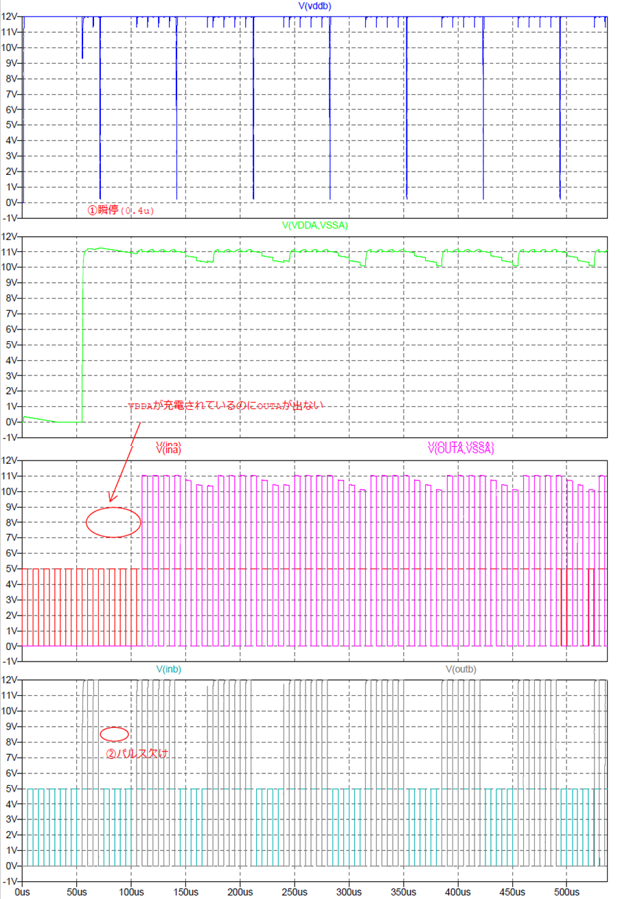
Between 30 and 60 usec after applying voltage to VDDA,

Even if a pulse is input to VINA, it is not output from VOUTA.

· Is this behavior based on the specification of UCC 21520?

· If this answer is 'yes', can you tell me the reason?

※Verification circuit diagram and waveform result are also attached

Verification Circuit

Waveform

Best regards,

Masumi Sekigcuchi

  • Hello Masumi-san,

    Thanks very much for your message.

    Yes, the bahavior "Delay from VDDA/B (above UVLO) to OUTA/B is around 50us" which is used to filter out unexpected VDD oscillation and accident turn-on. It is suggested to launch the PWM INput after 100us when VDDs ready (above UVLO). However, the UVLO off delay is very small less than 500ns, depending on VDD turn-off speed and steady state turn-off voltage, 0V or other value below UVLO .

    Btw, can you please help me understand why the VDDB show a lot of glitches?

    Please feel free to let me know if you have any further questions.

    Wei

  • Hi, Well-san.
    Thank you very much for the answer.

    By the way, can it adjust without delay time(50 usec)?
  • Hello Masumi-san,

    The 50us cannot be adjusted externally. However, it can be avoid by proper managing VDDA. See the image below for your references.

  • Thank you for your answer.

    Is my understanding OK that proper managing be below?
    (It is my understanding from the image ....)
    · Launch VDDA with a slope
    · Do not drop VDDA below UVLO after VDDA is started up
  • Hello Masumi,

    Thanks very your questions to confirm.

    The schematic you shows to me has boostrap for the high side VDDA power supply. Therefore, to have VDDA, we should have INB and OUTB to charge the VDDA first. We typically don't launch VDDA, it was boostraped shown in the schematic from VDDB to VDDA through D1. After the VDDA over UVLO threshold, wait for 100us, then both the VDDA and VDDB is ready, and then PWM INA and INB can start and OUTA and OUTB will follows properly.

    Wei