This thread has been locked.

If you have a related question, please click the "Ask a related question" button in the top right corner. The newly created question will be automatically linked to this question.

SN65HVD1473: Ackward RS-485 Weveforms.

Part Number: SN65HVD1473
Other Parts Discussed in Thread: TIDA-00892, ISOW7841,

Hi everyone,

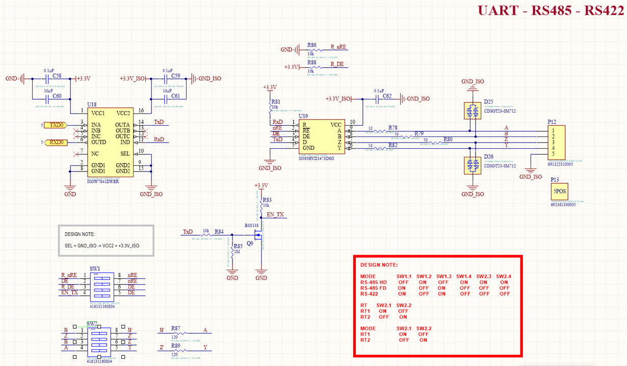
I'm checking a design, that it's basically this evaluation board with some adds to add RS-485 Half-Duplex and RS-485 Full-Duplex and RS-422 support: 

I' had to build a prototype because the evaluation board was not available. I was asking some questions related to this issue in this post:

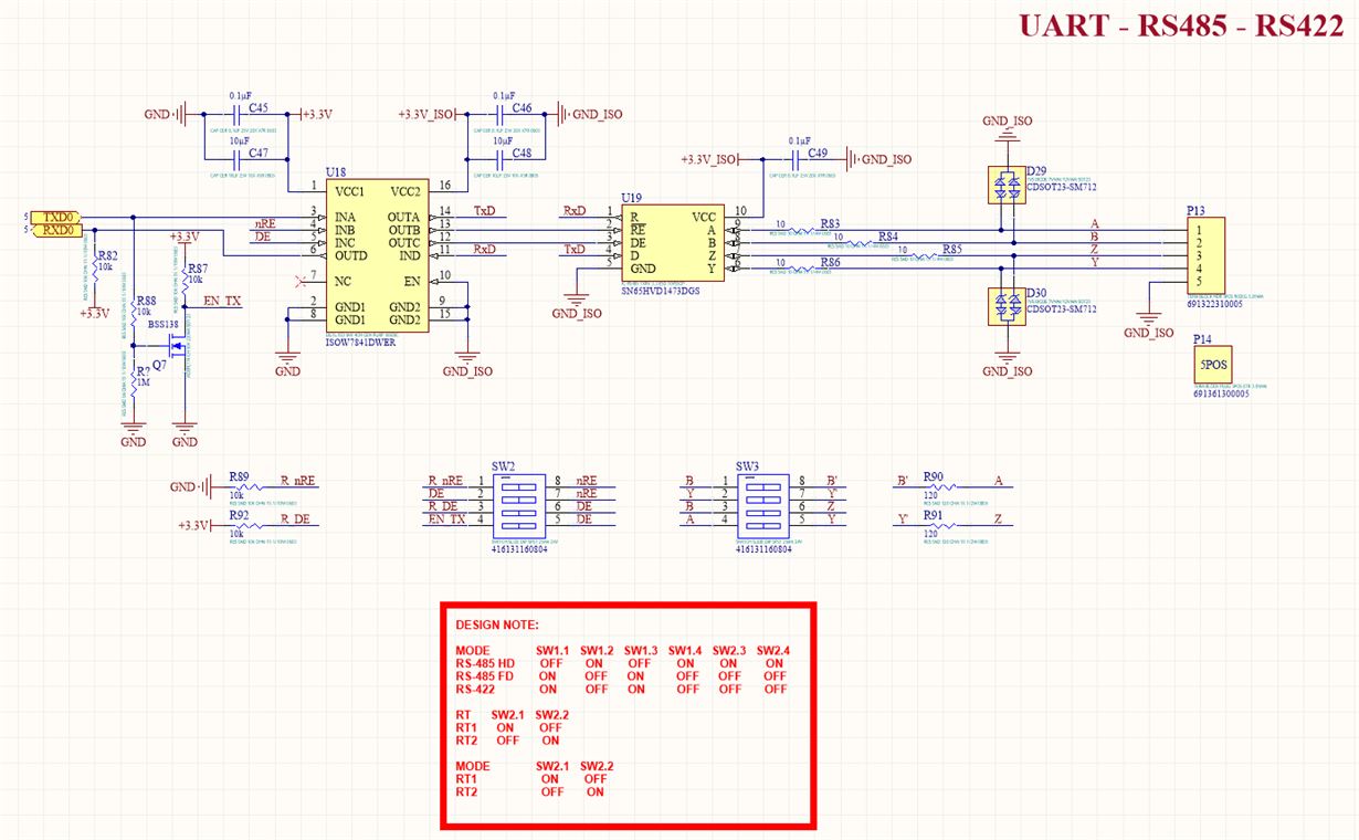
I attached my current schematic:

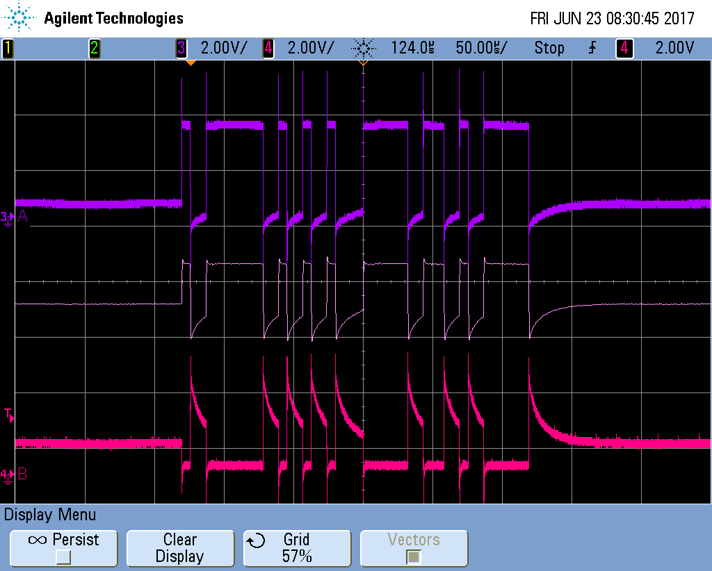
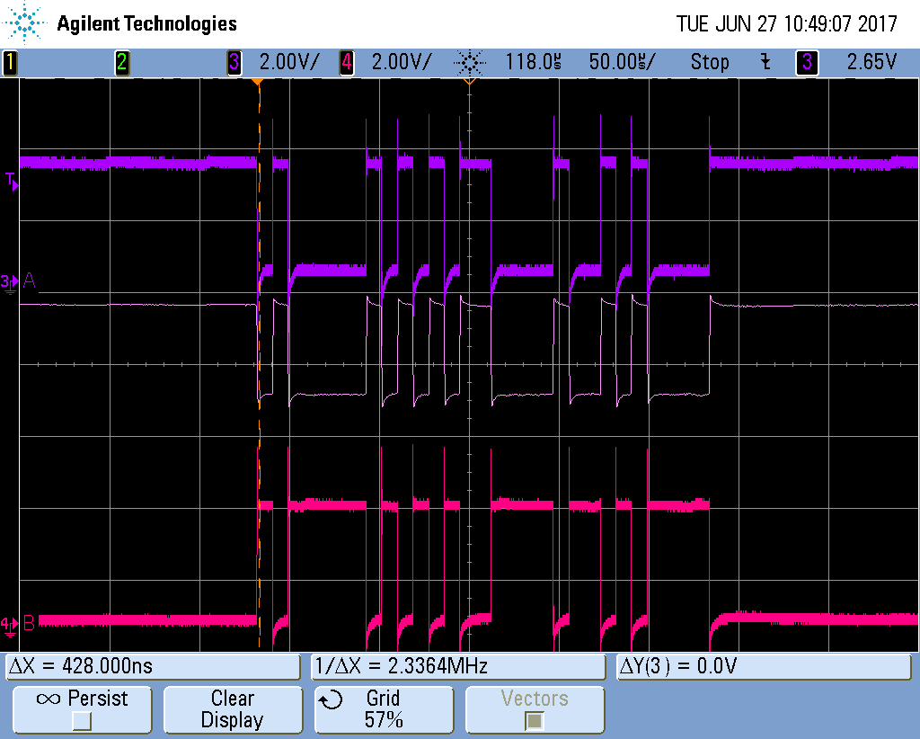
The design it's working fine until 230000 bauds. But I was analysing the waveforms and they look a bit weird. I don't have too much experience with RS-485 waveforms. I attached you the waveforms of the transmission/reception of a character "A". In this screenshot of my oscilloscope, you can see the signal A, B and in the middle is the math operation = A -B.

My questions are:

1.1.- Do you know if these waveforms are ok? The communication is working fine. I'm using the configuration in RS-485 half-duplex:

SW1.1 = OFF, SW1.2 ON, SW1.3 = OFF, SW1.4 = ON, SW2.1 = OFF, SW2.2 = ON, SW2.3 = ON, SW2.4 = ON.

SW2.1 = OFF, SW2.2 ON, SW2.3 = OFF, SW2.4 = ON, SW3.1 = OFF, SW3.2 = ON, SW3.3 = ON, SW3.4 = ON.

1.2.- I've tried to place the resistor termination of 120 Ohms and it doesn't work, so I don't place the resistor termination of 120 Ohms. I think with only 2 devices on the bus it's nor going to be necessary, isn't it?


2.- This IC SN65HVD1473DGS is failsafe biasing? or Do I have to add some extra components for that? According to this Application Note:

SN65HVD7x family and SN65HVD7X don't require an external bias resistor network. but I don't know what happen with my part number. 


Best regards.

  • Hi Oscar,


    Good to hear from you.

    First off I am assuming SW2 is SW1 in your design note as is SW3 being SW2.

    You have a 3.3_ISO power supply on your schematic. Is that just for the net label because the ISOW7841 provides an isolated 3.3V on Vcc2 when EN is tied to ground?

    1.1   These waveforms are a bit odd. The A and the B line should be the inverse of each other but the same amplitude.  You seem to be having a lot of ringing and attenuation of the B line. Off the top of my head you might be running into impendence mismatch.

    1.1.1          Are you putting your scope probe ground on the same ground so you don’t break the isolation you have?

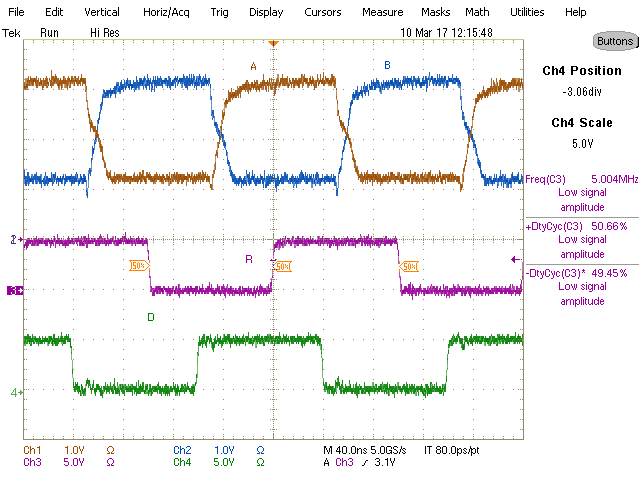
    1.1.2          Could you try tying DE high and sending the same data through the D pin, to see if the signals clean up? Ideally they should look like something close to this.

    1.1.3          Do these signal look this bad at lower data rates?


    1.2   When you say “it doesn’t work” do you mean the whole system stops working or the signals do not get better?

    1.2.1          Because if the whole system stops then there is a bigger problem.

    1.2.2          You should have the 120Ω termination resistor on both transceivers or you will get reflection on the bus because you are not impedance matched. So if you are transmitting and receiving on the same board you should have a 60Ω resistor to simulate two transceivers. 

    2.1  As for failsafe biasing your RS-485 IC does have failsafe internally. You can see it in section 10.2.1.4 of the datasheet. You do not need any external components to make this work.

    I will be able to test your setup on Monday to try to replicate your results.

    Regards,

    Daniel Noel 

  • Hi Oscar,

    I had to order the parts. They will be in a few days.

    Regards,
    Daniel Noel
  • Hi Daniel,

    Thank you very much in advance for your quick reply and your help.


    1º. According to: "First off I am assuming SW2 is SW1 in your design note as is SW3 being SW2."

    Yes, you are right. I made a mistake.

    2º.- According to: "You have a 3.3_ISO power supply on your schematic. Is that just for the net label because the ISOW7841 provides an isolated 3.3V on Vcc2 when EN is tied to ground?"

    Yes, with EN(SEL pin) tie to GND, VCC2 = 3.3V (Isolated).

    3º. According to. "Are you putting your scope probe ground on the same ground so you don’t break the isolation you have?·

    I'm using the GND_ISO to get the waveforms not the GND, so I think I'm not breaking the isolation.

    4º.- According to: "Could you try tying DE high and sending the same data through the D pin, to see if the signals clean up? Ideally they should look like something close to this.":

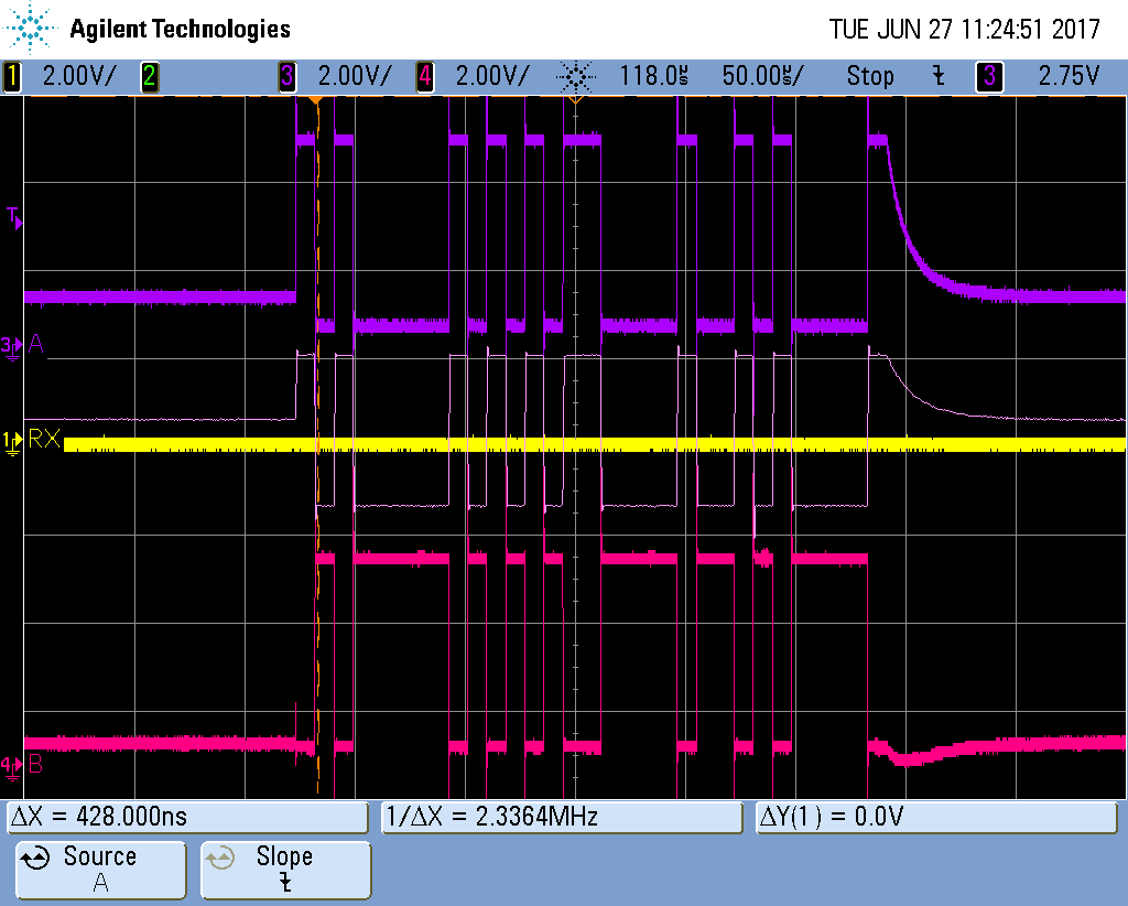
    SN65HVD1473 RX: When I configure the device like an RS-422 RX, the signals are quite clean. This is when I send the character A from a PC: "A\r\n":

    SN65HVD1473 TX: When I configure the device like an RS-422 TX, the signals are different than the RS-422 RX and they are similar to the RS-485 configuration. This is when I send the character A to a PN: "A\r\n":

    5º.- According to: "When you say “it doesn’t work” do you mean the whole system stops working or the signals do not get better?":

    To check everyting I'm usign a raspberry Pi, so when it's working I can see the messages from the console.

    Regards,

    Oscar Gomez Fuente

  • Hi Daniel,

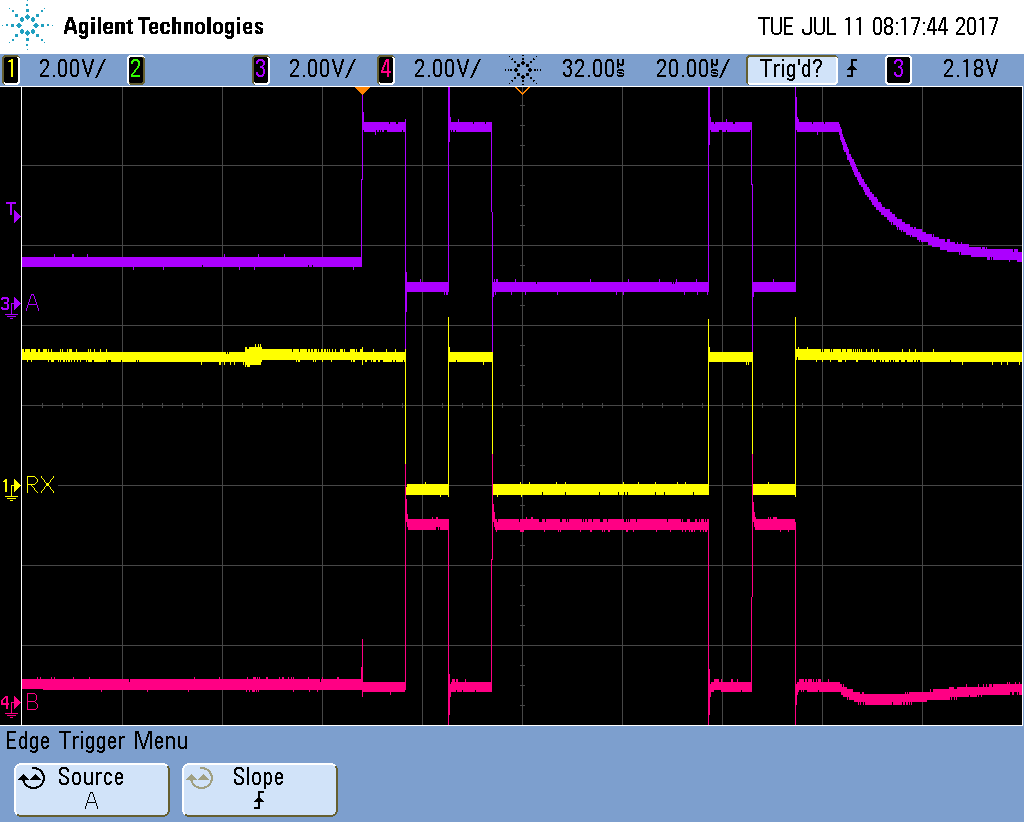
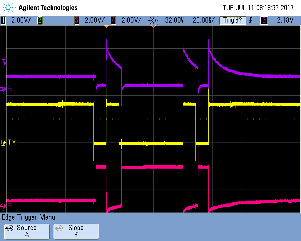
    I made more tests. This is the waveforms in RS-485 mode:

    RX ("A\r\n"):

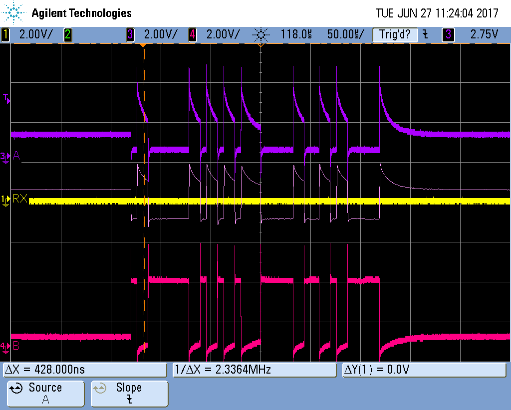
    TX ("A\r\n"):

    So the problem it seems to be in the TX.

    Best regards,

    Oscar Gomez Fuente.

  • Hi Oscar,


    How are you creating the differential signal for the RX ("A\r\n"): picture? Are you using another RS-485 transceiver to end the data or simulating it on your pi?

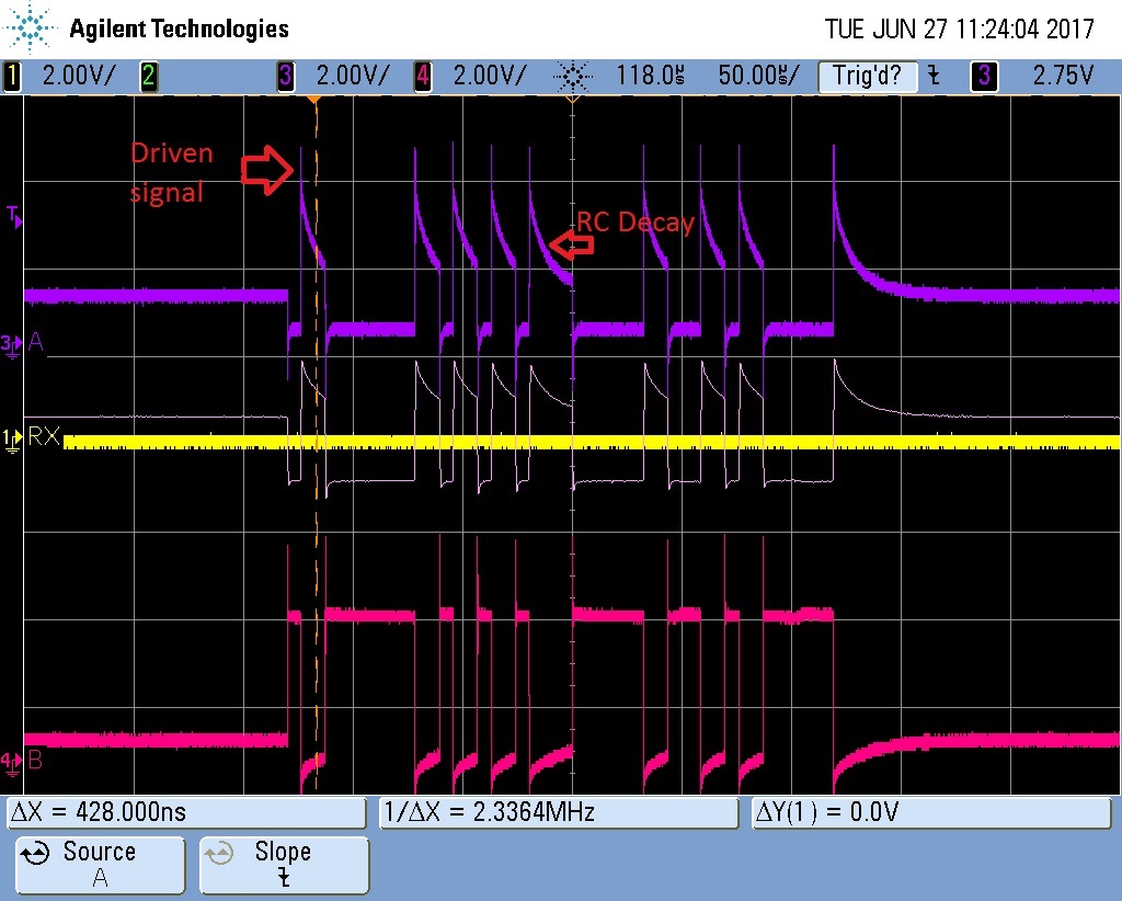
    For the second picture TX ("A\r\n"):, it looks like you are driving a signal on D (which is the spike) and then a short time later the MOSFET pulls low disabling the driver and then the device try’s to settle to the built-in failsafe voltage (the RC effect). The time difference is probably due to the capacitance of the MOSFET and this would become prominent at higher speeds. You can see on the last bit, the device settles to its voltage.

    You could try to offset this effect with external failsafe biasing to try to get better margin so the voltage doesn’t have to drop that far when the driver gets disabled.

    Are you still receiving data? Because you show RX=0V


    Regards,

    Daniel Noel 

  • Hi Daniel,

    I'm sorry for these messy pictures. I'm trying to do several things at the same time and definetely I can't.

    You have to ignore TX signal (I forgot to OFF it in the oscilloscope) and the pink signal is a math operation = A - B.

    But I'm going to capture the signals again, and I'm going to include RX and TX. I hope to take that as soon as possible.

    Best regards.
  • Hi Daniel,

    I'm sorry for the delay, but I was very busy.

    I attached the schematic again. I made some changes and I build a new PCB (I tried to avoid some errors in the last one). I place the SW1 and the MOSFET for Enable/disable the TX/RX after the isolator in order to check something different (Do you think is better to place this electronic after or before the isolator?):

    I was checking the RS-485 Half-Duplex mode, so SW1:

    SW1.1 = OFF -> Pull-down resistor on nRE pin disconnected.

    SW1.2 = ON -> DE and nRE tied together.

    SW1.3 = OFF -> Pull-up resistor on DE pin disconnected. 

    SW1.4 = ON -> EN_TX tied to nRE and DE pins together.

    and SW2:

    SW2.1= OFF SW2.2 = OFF -> NO termination resistors. I only have two devices in the bus with only 1 meter of distance.

    SW2.3 = ON -> B and Z tied together.

    SW2.4 = ON -> A and Y tied together.

    This the screenshot of the RX [Speed 115200 bps and I sent the character "A"]:

    And this is the screenshot of the TX [Speed 115200 bps and I sent the character "A"]:

    So I think the problem is in the TX... Any suggestion?

    Best regards.

  • Hi Oscar,

    Could you try sending the signal without using the mosfet. Such as tie DE high and transmitting on the D pin with and without termination? I think you might be running into speed limitation of using the disable/enable switching scheme.

    Regards,

    Daniel Noel

  • Hi Daniel,

    Thank you very much for your help and quick reply. I'm really stuck.

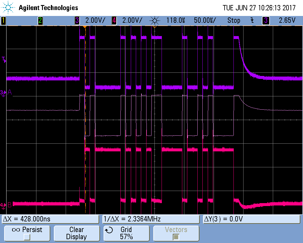
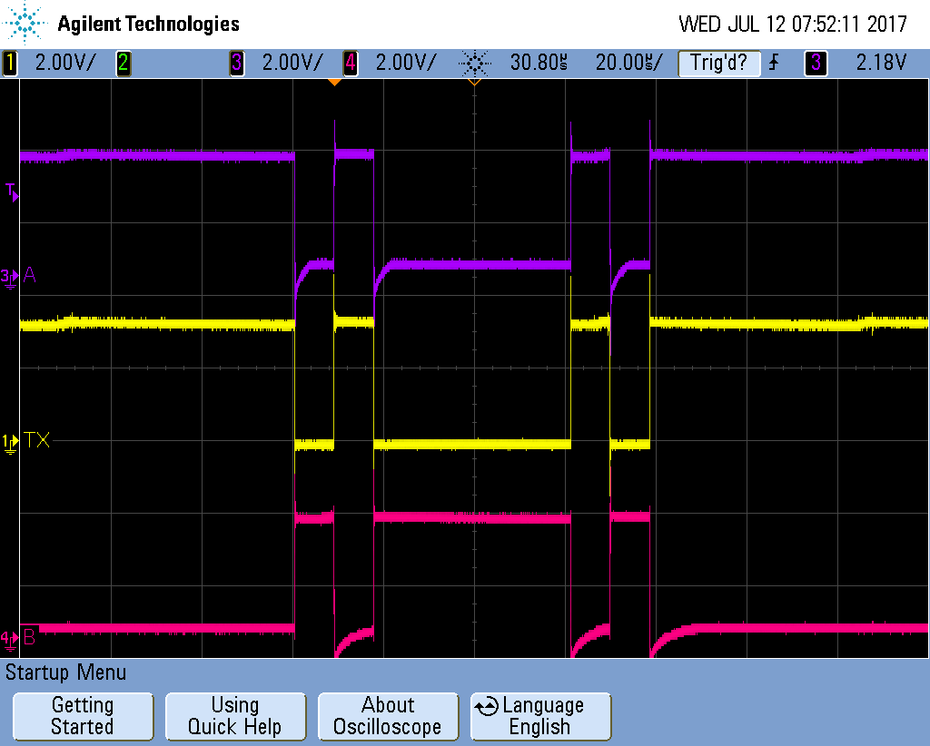
    First of all, I forgot to tell you the speed I'm using: 115200 bps. So I think it isn't a speed problem. This is the screenshot with nRE=DE=High and I sent the character "A":

    Best regards.

  • Hi Oscar,

    The signals look a lot closer to standard RS-485. Which would lead me to think that the mosfet is turning DE off just after D goes high and then the A line decays down to the built-in fail-safe voltage.

    The over shoot on the failing edges on A and B from your most recent post is probably due to reflections on the line since (I assuming) its not terminated. You could try to run is at a faster data rates to see if signals look like they did before.

    Regards

    Daniel Noel