This thread has been locked.

If you have a related question, please click the "Ask a related question" button in the top right corner. The newly created question will be automatically linked to this question.

TPS25741: Design with 4-Switch Buck / Boost Converter PMP10698

Part Number: TPS25741
Other Parts Discussed in Thread: PMP10698, , TPS65981, LM5175, , TS3USB30, TPS65982, TPS65982-EVM, TPS65986EVM, DP-EXPANSION-EVM, USB-CTM-MINIDK-EVM

Hi All,

I am new to USB-C design. I am currently designing a board that will do data transfer (max 480Mbps), and supply full power delivery (100W). I am using the PMP10698 reference design for my buck-boost converter to essentially provide 5/12/20V @5A.

The TPS25741 will use the CTRL1/2 lines to set the output voltage based on its negotiations. It explicitly says in the datasheet that it does not communicate with the cable to determine its type? My worry is someone will plugin a 3A usb-C cable and my device will attempt to put 5A through it. How can I check the cable type? Am I using the wrong USB-PD controller? I really like the ability to have one buck-boost design provide all 3 levels.

Thanks in advance,

Kai Rasporich

  • So I think its probably best if I use the TPS65981. Can someone please advise if this works with the PMP10698? Is the chip configured via software to advertise the proper voltage levels?

    Thanks,

    Kai

  • Hello Kai,

    We have the attached design using TPS25741. But, to answer your last question, TPS65981 could also interact with LM5175./cfs-file/__key/communityserver-discussions-components-files/138/0576.PR2254E2_2800_Variant-of-TPS25741-Referecne-Design_29005F00_Sch.PDF

  • Hi Eric, 

    Thanks for the reply. My question is actually whether or not the TPS25741 is able to detect the cable and adjust its current advertisement accordingly? I have reviewed the schematic you posted, I do not see the TPS65981 in the schematic, but I am assuming the CTL1/2 pins out of the LM5175 go into a GPIO of the TPS65981. Perhaps it is the wrong schematic?

    Thank you for your help!

    Kai

  • Hi Kai,

      TPS25741 cannot tell whether the cable is 3A or 5A. If using the TPS25741 in a 5A application, the cable should always be attached to the terminal (captive cable). 

      TPS65981 adjusts the frond-end AC/DC or DC/DC trough toggling the GPIOs, same as TPS25741.

    Regards,

    Patrick

  • Thanks Patrick,

    Is there any other downsides to using the TPS25741 over the TPS65981?

    Kai
  • Hi Kai,

    TPS25741 is the simplest part to achieve PD charging with data within 60W(100W wiht captive cable). It does what it does and requires no firmware.
    While TPS6598X is a more flexible yet more complicatied part(also more expensive). It enables DRP, e-marker cable communication, video, etc..
    I wouldn't call TPS25741 has downsides over TPS65981. it's just they have different level of integration and therefore target different applications. May I ask what particular applicaiton you're aiming for?
    Thanks.

    Regards,
    Patrick
  • Thanks, I think the TPS25741 is what I am looking for. We essentially have an ATMEL SAMA5D31 processor, and we are using the ports mainly for power delivery. The USB protocol will only be 2.0. Based on what you have said, and what I have researched. I think the TPS25741 is a better choice, given we will also have 3 Ports capable of full 100W PD. We won't be transmitting video etc.

    So maybe my solution is this, could I have a jumpers between HIPWR and GND, HIPWR and DVDD, so that we could select whether 3A or 5A is advertised? This might be a dumb question... but will the TPS25741 limit the current from the LM5175 configuration based on the state of HIPWR?

    Thank you so much!

    Kai
  • Hi Kai,
    You're absolutely right that you can use jumper to set HIPWR for advertising different current abilities. And the device will set its own current limiting based on your setup. One more suggestion is that you can refer to TPS25741 datasheet and EVM user guide for jumper configuration, because there're more information about the HIPWR(pull high through res, pull down through res). Thanks.

    Regards,
    Patrick
  • thanks, I think I actually decided I will use the TPS65981 for the port that can be both device and host (OTG), and use the TPS25741 for the other two ports!
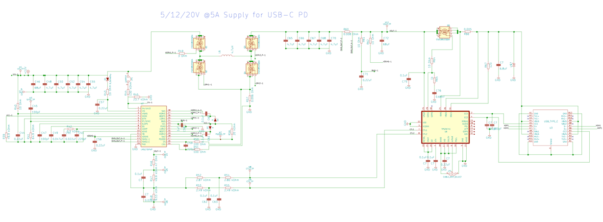
  • Would someone be able to look this over for errors? This is my design so far using the TPS25741.

    Thanks in advance,

    Kai

  • Hi Kai,
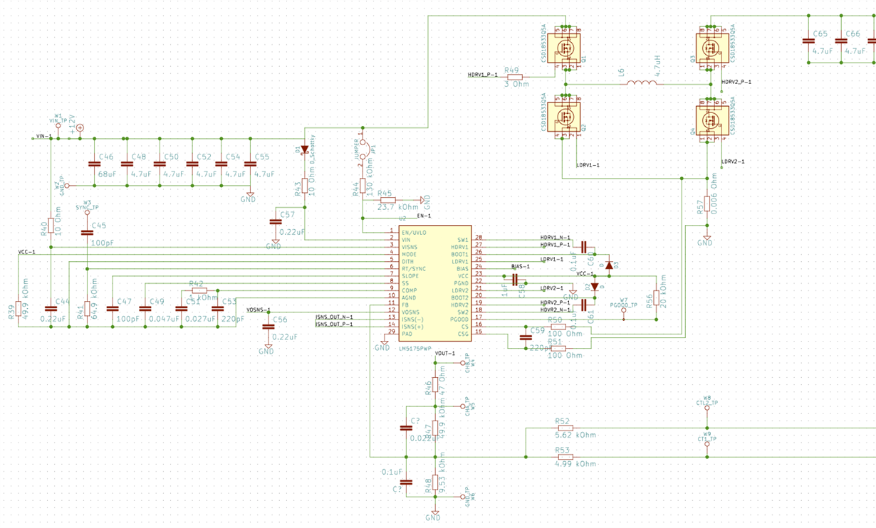
    Generally, your schematic looks good. It looks like you've used PMP10698 for the power supply which is fine. In PR2254E2 (earlier attachment I sent), we've changed a few component values such as the LM5175 COMP pin zero (1k and 0.027uF) and also the slew caps around the FB pin (upper should be 0.022uF and lower = 0.1uF). You could also combine the CTL1/CTL2 resistors into one value as shown in PR2254E2 (the "T" network is replaced by the slew caps around FB. Pin programming of the TPS25741 looks good (93W at PSEL and 5A or 3A at HIPWR).

    The current sense resistor value showed as 8 milli-ohms rather than 5 milli-ohms and I'd recommend using the R-C filter on Rsense for starters (you could remove it later if not needed). The CC1 and CC2 caps show as 300pF. We'd recommend 470pF. There is only one FET which is OK for a captive cable design but blocking of the LM5175 bulk capacitance is required if using a receptacle. For the Back-back FET design, see PR2254E2.

    The schematic is a bit fuzzy so I may have missed some values. Please attach a PDF if possible for the next round.
  • Hi there,

    Thanks for reviewing the schematic. I made the changes as per your recommendations, see attached screenshots. I have a few questions:

    1. Should the ISNS+- pin on the LM5175 be connected?

    2. What is the purpose of the smart diode on the PR2254E2? Would you recommend I include it?

    3. Is it ok I am powering the TPS25741 off of the VPWR pin and not VCONN?

    4. PR2254E2 shows diodes D6/D7 (3.2V) attached to the main bus, what are their purpose?

    5. As I understand it, the pins "DEBUG,AUDIO,POL,UFP,GDPG,G5V" are for debugging, is this correct? They are not needed to operate the chip? Would you recommend test points on any of them?

    Thanks!!

    Kai

  • Hello,

    1. Should the ISNS+- pin on the LM5175 be connected?  ISNS+ and ISNS- may be either connected together or connected to ground is this function is not used.

    2. What is the purpose of the smart diode on the PR2254E2? Would you recommend I include it? Your application may not need reverse input voltage protection.

    3. Is it ok I am powering the TPS25741 off of the VPWR pin and not VCONN? There is a "VCONN" switch inside the TPS25741 to apply 5V to the opposite CC line if required. The VCONN pin is the input side of the internal switch. If you don't need the VCONN switch function you can connect VCONN to GND (it is not a power supply input to the TPS25741).

    4. PR2254E2 shows diodes D6/D7 (3.2V) attached to the main bus, what are their purpose? These are just LED's for the user and are not required.

    5. As I understand it, the pins "DEBUG,AUDIO,POL,UFP,GDPG,G5V" are for debugging, is this correct? They are not needed to operate the chip? Would you recommend test points on any of them? DEBUG, AUDIO, POL, and UFP are status outputs which depend on what is connected via the type C connector. We use the POL signal to select which channel of the high speed mux is used for data. UFP is a signal which is active when a sink is connected and can be used for certain functions but is not always req'd. G5V and GDPG are extra gate driver outputs which can be used in power muxing applications (see TPS25741EVM-802 user guide).

  • Thank you for the detailed reply.

    I have one more question! More on the data side of things, given that D+- pairs are on both sides of the connector. Would I also need TS3USB30 High-Speed USB 2.0 (480-MBPS) chip in order to multiplex the signal, based on what the POL signal is? Is this the proper way to do it? I see that the TPS65982 has this functionality built into it.
  • These can just be hard connected under the type C connector (no mux needed) as shown on PR2254E2
  • Hello,

    I have decided to use the one design with the TPS25741, and one port with the TPS65986, would you be able to post an evaluation board schematic for the TPS65986 if one exists? Similar to what you sent me for the the TPS25741.

    Thanks!

    Kai

  • Hello Kai,

    Did you get a chance to look at any of these designs on the TPS65986 Tools Folder? Please have a look here: http://www.ti.com/product/TPS65986/toolssoftware

    Design kits & evaluation modules (4)

    NamePart#Type
    TPS65982 USB Type-C & USB PD Controller Power Switch & High Speed Multiplexer EVM TPS65982-EVM Evaluation Modules & Boards
    TPS65986 USB Type-C & USB PD Controller & Power Switch Evaluation Module TPS65986EVM Evaluation Modules & Boards
    TPS6598x DisplayPort Expansion Evaluation Module DP-EXPANSION-EVM Evaluation Modules & Boards
    USB Type-C™ Minidock Board With Video and Charging Support Evaluation Module USB-CTM-MINIDK-EVM Evaluation Modules & Boards

    There is also a reference design that may suit your needs.

    http://www.ti.com/tool/TIDA-01243

  • Hi Eric,

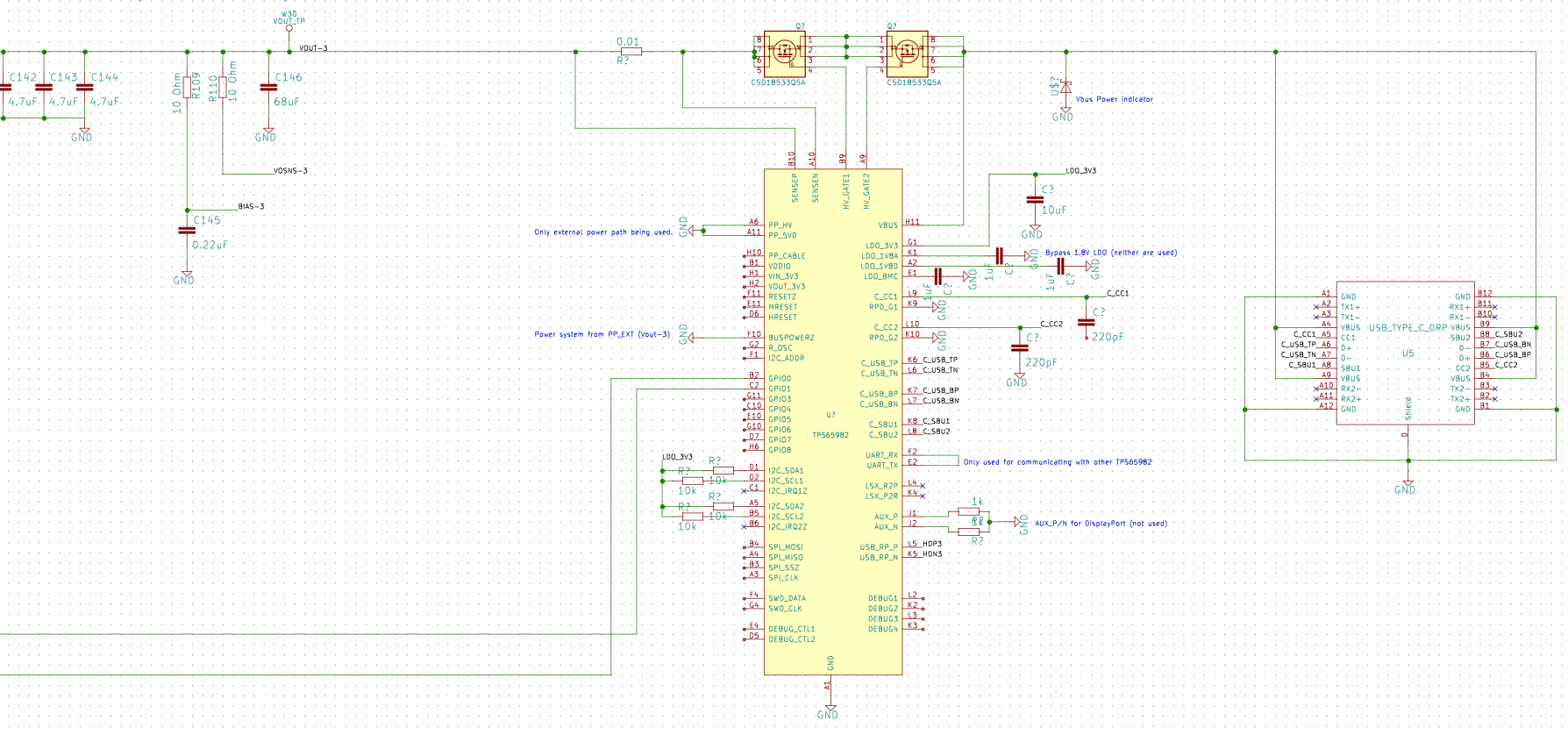
    I am now working on the design for a USB port using the TPS65982. I have a few questions I hope you can assist with:

    • As I understand, the TPS65982 is able to be powered off of Vbus, if this is the case, should my Vbus connection actually connect before the gates? Since there would be no power after the gates, unless a cable was plugged in?
    • Is the external flash absolutely necessary? I am only using 480Mbps USB D+/-, and providing external power via the LM5175 circuit as previously shown.
    • What is the best method to communicate with the TPS65982 for programming? I will be needing to program it to control GPIO 0/1 to control the voltage output of the LM5175 circuit.

    Thanks!

    Kai

  • Hi Kai,

    1) see screenshot below for VBUS location clarification for the 82. VBUS is connected after the FETs.

    2) Yes external flash is nessessary, The TPS65982 firmware is divided into two sections: boot code and application code. The boot code is responsible for configuration of the device immediately after power application. The boot code is stored on internal device memory and cannot be altered. The TPS65982 application code is stored externally, and is loaded by the boot code.

    3) If you want to control buck-boost with GPIO0/1 event you can use 'GPIO event map' (0x5c) in the config tool to select the event you wish to trigger the different output voltage.

    Please let me know if this helped you or you need more assistance!

    Thanks!

  • Thanks Jeff,

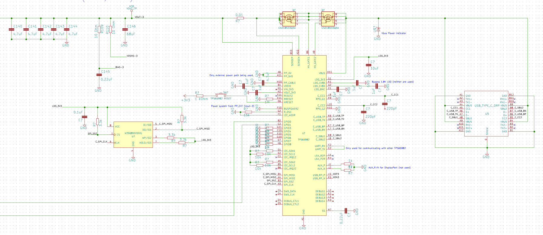
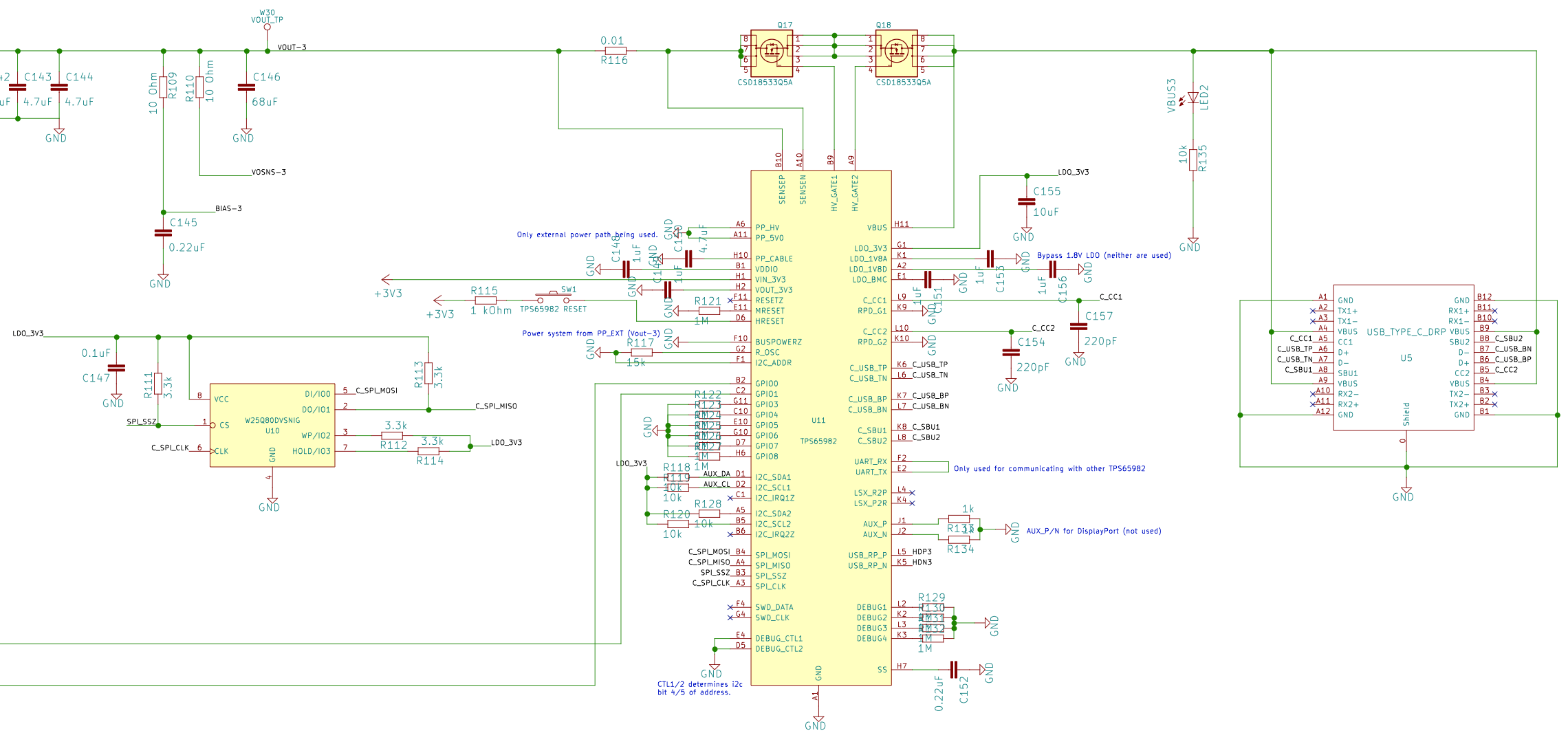
    That clarifies a lot for me. Is it possible then for me to have the TPS65982 only powered off of the external VBUS supply? Or will I need to supply 3.3V to the VIN_3V3 pin? I have attached a screenshot of my schematic so far. To the left is the 4-Switch Buck/Boost Converter Schematic, supplying the 5/12/20V @5A.

    As well, what is the best protocol to program the TPS65982, should it be hooked up to my main processor via i2c?

  • Here is a more detailed view of the schematic. Does this seem ok? 

    • I am unsure regarding the actual communication between the TPS65982 and my main processor. I currently have it hooked up via i2C.
    • Can I tie together the GPIO pins not being used through the same resistor, or do they need to be separate grounded through the 1M resistor?
    • I am using the reference design HVL117D, and they show a 21ohm resistor, and 4 0.01uF caps in parallel on the Vbus line, would I also need these? I have an array of capacitors on the other side of the FETs already.
    • Will the TPS65982 run off only VBUS power, or is an external 3.3V regulator needed to supply VIN_3V3?

    Thanks again for your help! I realize these may be dumb questions!

  • Hi Kai,

    1) It is possible for the 82 to be powered off of VBUS.

    From the 82 datasheet on ~pg70

    1a) The 82 will use VIN_3v3 or VBUS to Initialize and configure i2c. After this the 82 checks VIN_3v3 to determine cause of boot. If the 82 is booted from a source other than VIN_3v3 the dead battery flow is followed to route the appropriate power path for dead battery operation.  

    1b) VIN_3V3 takes precedence over VBUS, meaning that when both supply voltages are present the TPS65982 will power from VIN_3V3.  There are two cases in which a power supply switch-over will occur. The first is when VBUS is present first and then VIN_3V3 becomes available. In this case, the supply will automatically switch-over to VIN_3V3 and brown-out prevention is verified by design. The other way a supply switch-over will occur is when both supplies are present and VIN_3V3 is removed and falls below 2.85 V. In this case, a hard reset of the TPS65982 occurs prompting a reboot.

    2) You can directly R/W to registers from your main processor via i2c. I can give you more detail if needed.  

    Thanks

  • Hi Kai,

    I will review your schematic and get back to you asap.

    Thanks
  • Thanks Jeff, I have changed the design to also provide a 3.3V supply to VIN3V3. 

    Thank you again for reviewing the schematic, I really appreciate the customer service and support that TI provides for their products.

    - Kai

  • Hi Kai,

    Thats what I am here for. Ask away.

    1) do you require to control the 82 from an EC via i2c? 

    e2e_QA_TIDA_82.docx

    Thanks

  • Thank you very much. I will post an updated schematic, and I am hoping you can catch any errors you might see!

    Kai
  • Hi Kai,

    Will do, I will compare your schematic against our EVM to see if your differences will work. Ill update u asap.

    Thanks
  • Hi Kai,

    I attached a word doc to give you my observations. Your connections and recommended capacitance looks ok. Please let me know if you have any more questions!

    sch review TIDA_82.docx

    Thanks

  • Thanks for the Feedback Jeff. I made those changes as per your recommendations!

    Kai