This thread has been locked.

If you have a related question, please click the "Ask a related question" button in the top right corner. The newly created question will be automatically linked to this question.

SN74AVC32T245: Require layout example for voltage level translator

Part Number: SN74AVC32T245

Dear Sir/Madam,

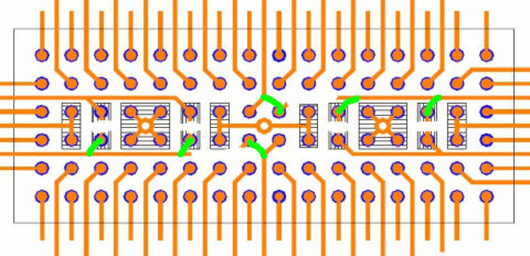
In SN74AVC32T245 datasheet figure 14, provided layout diagram will only match for 32 buffer/driver routing. Since it uses only single supply. Kindly provide layout diagram for voltage level translator where two supply are used VCCA and VCCB.


  • That figure was simply copied from the SCEA14 application report.

    You will have to route two of the center balls (H/J-3/4) through a via so that you have space for the two additional VCC traces.

    But if the four xDIR and xO̅E̅ signals are tied together, you need fewer traces and can avoid those vias; see the changes below if 2DIR=3DIR and 2O̅E̅=3O̅E̅: