This thread has been locked.

If you have a related question, please click the "Ask a related question" button in the top right corner. The newly created question will be automatically linked to this question.

TXB0104: issue with voltage translation and GND connection

Part Number: TXB0104

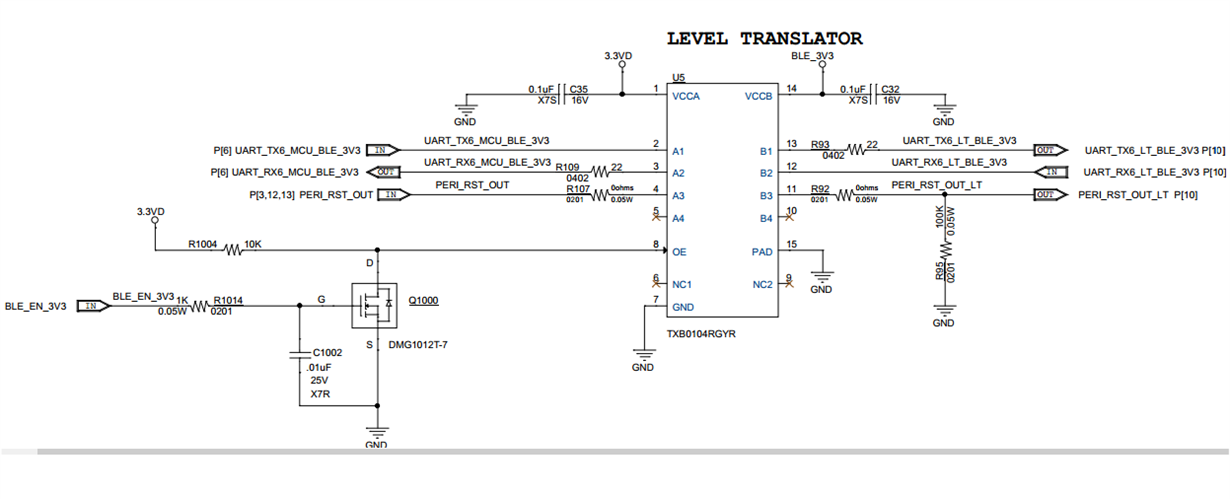
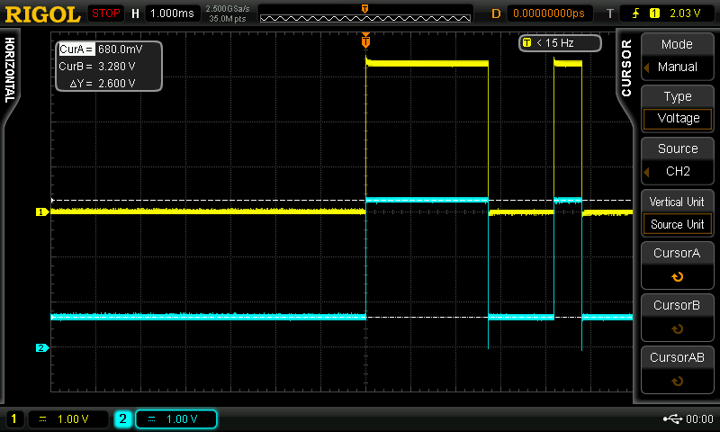
Hello , we are using TXB0104 IC in our design in RGY package for UART signal voltage translation. In our design we are seeing that  the voltage on B side is not  proper for one of the signals Please see below picture , the issue i am pointing out is with signal observed on pin13 

THe waveforms of Pin2 (Yellow) and Pin 13 (Blue) are shown below :-

 I have following questions 

1. If you see the waveform at pin 13 , it is not at zero volt really even when the Input side signal at pin 2 is at zero Volts. As recommended in datasheet of TXB0104 , we do not have any pullups  or pulldowns on either B side or A side. Our signal driver on A side for pin 2 is of push pull type .So why does the level at pin 13 side not proper ?

2. WE have left floating the pins 5 and 10 , though this is not recommended , but i believe that is not an issue causing improper levels as per point 1 above since anyways there is a weak driver on each side of the TXB0104 and once one side is latched to a high or a low , the other side should continue driving the same. Is it not ? 

3. WE have also connected the exposed GND PAD under the IC to our board Digital GND ( common to both input and output side of this translator) - is that the issue behind the improper levels we are seeing as per point 1 

We are ensuring in our design that the OE pin of the translator  is driven low at power up and only when required , it is drive high during data transmission.

Regards

jitender

  • Jitender ,

    what is the loading on the output , having larger cap load could possibly cause this coupled with a weak process device. usually, the higher the frequency the 'low' voltage can get gradually higher, although this case the frequency is not high. Is there a reason for using this for buffering instead of a conventional buffer ?

  • I would advise A4 and B4 to be at gnd.
    What about A3 and B3 signals ? you have a pulldown 100k on B3 , does this signal trace have a problem going low ? what about removing the 100k pulldown and probing it again ? I tried simulating the IBIS model and with low freq there is no problem to have the line go low.
  • hi shreyas,
    1. the loading on pin 13 is quite less - about 2 inches of trace and one single load - a BLE transcevier probably having pin capacitance of 10pF .
    2. if you see our schematics , we have the two sides of buffer powered with two different rails . A side rail voltage is always available and B side rail voltage can be switched ON and OFF based on whether the bluetooth module needs to be active or not.

    the frequecy of these signals is 4800 / 9600 bauds - so it is quite low.

    regards
    Jitender
  • Hello shreyas,

    Yes, we will connect A4 , B4 to GND , however i suspect that may not solve the issue. I had seen another post regarding this where it was suggested thatdue to internal latch like action it may not be an issue to leave these pins floating . Hwever in any case tomorrow , i will try after connecting both A4,B4 to GND

    A3, B3 are static signals and either remain at high or low level, the pull down shown in the schematics has been removed and post that i do not see any issue with A3,B3.

    Regards
    Jitender
  • I have now connected both A4 and B4 to GND , however i do not see any change in the signal observed at pin 13. Still the Low level is close to 0.7V.
    Does this have something to do with Grounding of Exposed PAD on the bottom side of the IC ? As i mentioned in my first post, it is connected to board common ground. In any case how can this have an efffect on signal level on only one specific signal ?
  • Jitender ,

    The I/Os to be connected to gnd is a recommendation we do for all the CMOS devices and not necessarily which helps to fix this issue.
    Exposed pad connected to gnd is another recommendation for mechanical /thermal stability.
    Is this problem repeatable when you replace another device from another lot ? Is this repeatable when you operate only this channel and disconnect all other channels ? Even with a large load (1kohm) , affects the high voltage (Voh) , however ,the low voltage will not be affected as long as it is operated at low frequencies.