This thread has been locked.

If you have a related question, please click the "Ask a related question" button in the top right corner. The newly created question will be automatically linked to this question.

LSF0204: down shift queston

Part Number: LSF0204

Hi Team,

After reading LSF0204 datasheet and app notes,

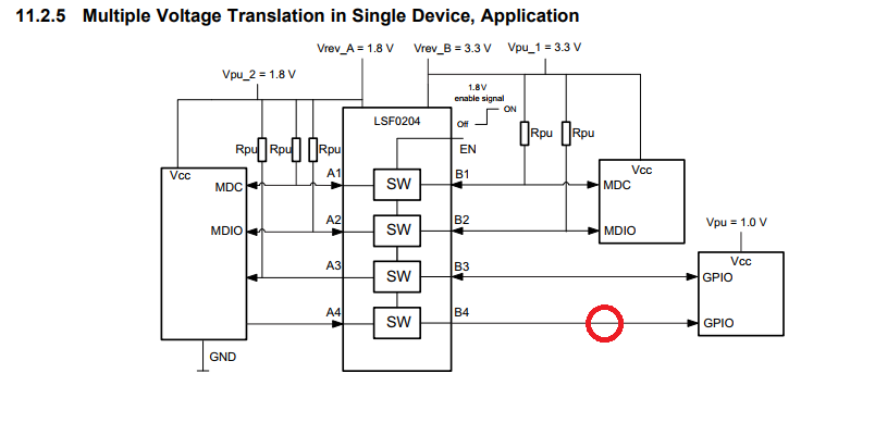
Where customer and I both cannot understand is why the red mark below don't need a pull up resistor?

Because the Vcc 1V is much small than Vref_B voltage. I cannot understand how this would work (I mean what voltage will appear at B4 pin?), please kindly teach me, thanks.

Andrew

  • Hi Andrew,
    Good catch. The way the circuit is drawn currently the signal on A4 would be directly transferred to B4, resulting in a 1.8V signal at the red circle. This was likely not the intent of whoever drew this circuit.

    There is an error in the datasheet. In order for this to work, the voltage at Vref_A would need to be 1.0V, and the wire connecting Vpu_2 to Vref_A would need to be removed (also, Vrev_A should be Vref_A...)
  • Thanks for the feedback!
    Can we just add an extra pull-up 1V at where red mark without changing Vref_A voltage?
    Will that work?
    Thanks.
    Andrew
  • Unfortunately, the LSF0204 will never be triggered with the thresholds set as they are (1.8V). If you have to come up with a work-around, one option would be to add a clamp diode to limit the 1.8V signal to 1V, but there would have to be a series resistor as well to limit current through the diode, and it kind of defeats the purpose of having a translator.

    The best solution is to set the reference voltage to 1V. All other channels will still work fine with the lower threshold.
  • This is exactly the thing I don't understand. Please allow me to ask more. How Vrev_A & Vrev_B works inside the device? If it acts as a pull up, then why needs additional pull up resistor? Thanks for teaching.
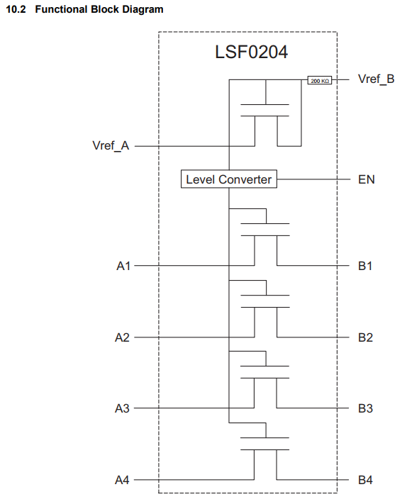
  • The datasheet has a very good block diagram in section 10.2

    The FET threshold voltage is set by Vref_A. Essentially, when any input is near the threshold (or above it), that FET will go into a high-impedance mode. When the input is below the threshold, the FET is turned on.

    In general, the above image explains how the LSF translators work.  In this image, the driver device is forcing the B1 pin LOW, which is causing A1 to also be low.  If B1 is forced HIGH, then the FET will become high-impedance, and A1 will be pulled to V_A through R_A1.

    I know this device family is a little hard to understand.  We are currently working on a video series to explain them better.

  • Thank you very much.
    In above (Inside the LSF) graph, the B side is on left, but in the datasheet block diagram the left side is A, do they mean to be same side or different?
    My understanding is that this device works the way that only allows current goes from right to left side, not the other way around, correct?
    Therefore, in above graph (Inside the LSF) , Vb should be lower than/equal to the Va + headroom.
    If voltage appears at B1 say 1.8V (pull up by Vb) is actually higher than Va say 1V, then Va will not be able to clamp the voltage for right side device.
  • The A and B sides are labelled correctly -- I swapped the sides for convenience in my drawing.

    Current can pass both ways through the LSF device.  The device is voltage controlled -- if (VG - VS) > Vtn, current will pass.  Since VG is a set bias value, VS is the only value that can affect the FETs state.

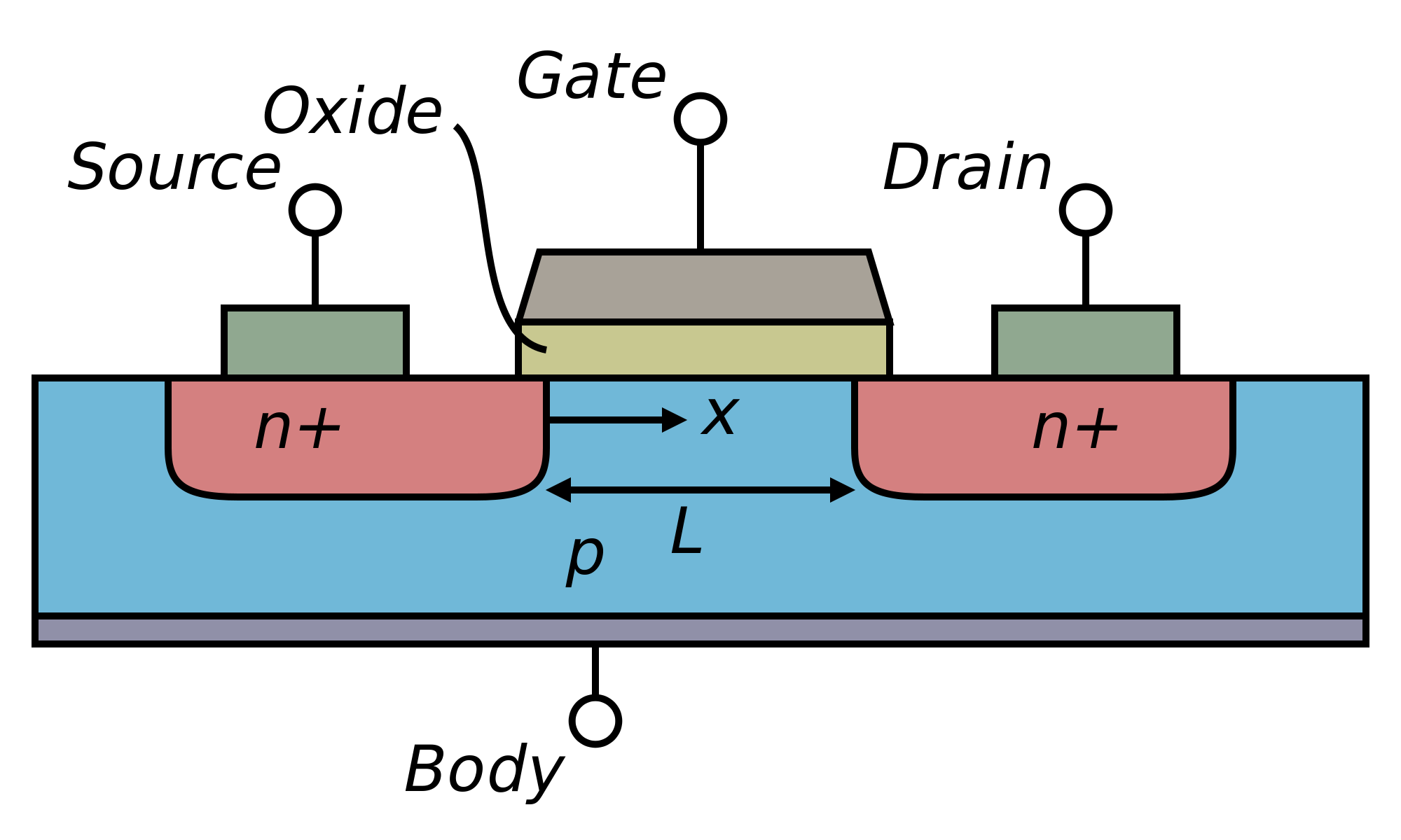
    The most confusing part of the device is that there isn't a set 'source' and 'drain' -- the 'source' is typically identified as the side of the FET that is shorted to the Body, but in this case, the Body is connected to ground, and the Drain/Source are symmetric.

    (borrowed image from https://electronics.stackexchange.com/questions/212768/p-chanel-mosfet-series-configuration)

  • You have been so helpful, nice article too, thank you very much.

    One last question (sorry), may I know what is Vref_B for? Vref_B voltage has nothing to do with pin B1~B4 voltage?

    Thanks!

    Andrew

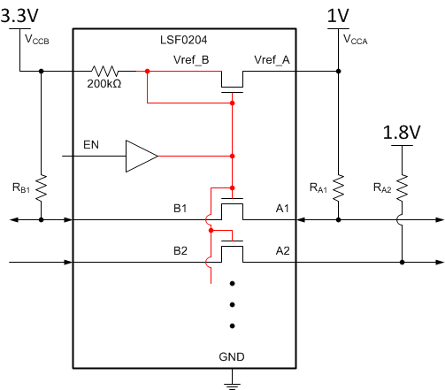
  • This internal schematic might make things a little clearer:

    ** One minor correction, Vref_B is the external pin name -- it should be labelled on the other side of the resistor.  Sorry for the confusion **

    Here you can see that the gate voltage (shown in red) for each channel is directly related to the bias voltage generated with Vref_A and Vref_B.

    This is why Vref_A must be set to the lowest voltage used with the device. Otherwise it will not work. This can be somewhat problematic in mixed voltage systems -- for example, a 5V signal line typically has a low voltage of anything below 1.35V, but a 1V signal would register as 'HIGH' if the threshold were set as shown above.  There are just some situations that won't work.

  • Thank you very much!!!

    Your graph really helps me to answer all my questions before!

    You are the man!! =)

    Andrew