This thread has been locked.

If you have a related question, please click the "Ask a related question" button in the top right corner. The newly created question will be automatically linked to this question.

TXS02612: SDIO Signal issue

Part Number: TXS02612
Other Parts Discussed in Thread: TS3A27518E

Dears ,  I have an SDIO signal issue when using this TXS02612 .  My simple DMAIC report is attached here . SCH is also provided .   In my design . the SD card is used to split out to 2 SD card ports in level one .  then a second TXS02612 is used in level 2 to generate another 2 SD card .   they are supplied by the same VCC3V3 .  

but I found that , when signal tranfer from port B to port A ,  there is a 0.8V decreased  .  I analyzed    it is not caused by the power sequence or  design . 

In case you can,t download the file , my summarize :

1,  Enable SEL pin  and design  is right ,  as we can see perfact signal from A to B0 .

2, power Sequence is not cause ,  as  I only  used TXS02612 , and  lead VCCA VCCB  SEL , data1A  data1B0 . the sequence and data direction  can be controlled by manual   .

3, signal from B0 to A , no problem .  using signal generator . 

can you help to confirm if there is some error that I missed . 

thanksTXS02612 SD Issue.pdf

  • Hello,
    I have asked our translation expert to take a look at this issue. He should be back with you soon.
  • Hi Emrys Maier
    is there any update~~ I really need your help . thanks
  • Hello,

    A few questions/clarifications, and I would be happy to help you with this. 
    Off hand, it is not clear to me exactly what might be causing this, but I will need to look into it further.

    1. Are you finding that this is the case for all parts or simply just one part?

    2. Is there any loading (load current) on the output of the device at the A side when you are trying to send data from B to A?

    3. Is the reference supply somehow getting pulled down?

    4. Have you tried doing a lower frequency data rate to see if the results have less attenuation?
    For example if you try a 1Mbps signal, does this have the same 0.7V drop? 

    Best,
    Michael

  • Hi ,Michael 

    thank you for your reply .  my answer here,  and can you re-do my experiments in your Lab using TXS02612 ? I think it is easy to do  if you have time .  Can you see my email in my profile , is it possible to contact you with email ?  thanks .

    1. Are you finding that this is the case for all parts or simply just one part?

     ------------all my PCBAs have the same issue ,  in order to identify what is the matter , I had Request 20 pcs of  TXS02612 from TI  Shanghai FAE .  Mounted some of them ,  the issue is still exist . 

    my SD controller is USB82642AM , but I tried other controller  ,  I think controller is not the cause . 

    2. Is there any loading (load current) on the output of the device at the A side when you are trying to send data from B to A?

    ------there is one test in the last page of my report  . I only solder some lead from IC ,  the IC is not on PCB ,   I just soldered out VCCA VCCB0 ,DATA1A ,DATA1B ,GND ,EPAD . using some leads .  supplying VCCA VCCB 3.3V

    you can see the pictrue in my report .   but the voltage is 0.7V different from input to output . 

    3. Is the reference supply somehow getting pulled down?

    --------No . in last question 2 , I stated an situation  ,

    4. Have you tried doing a lower frequency data rate to see if the results have less attenuation?

    -----------I tried an 150Khz frequency from signal generator .  the issue is still exist .(  0.7V )  even more , I tried VCCA,B =2.5 VCCA,B=1.8  ,there is voltage different  though it is not 0.7V . 
     

  • Hello,

    Yes, I will order samples of this device for us to evaluate. This will take a couple of days to get samples before we can evaluate on the bench.

    I will also work with a couple other contacts to see if they have seen this issue before. 

    Please allow a couple more days for us to look into this, and we should get back to you with follow up by Wednesday, and hopefully we will get samples to evaluate by weeks end.

    Best,
    Michael

  • Hi Wang ,

    Thank you for the reply.
    I was going through the report and i want some clarifications.

    Why do you have this device when you do not need translation as you are operating at 3.3V on Vcca /B0 and B1 ?
    are you following the power sequence as mentioned in the datasheet?
    Do you have 10k pullups on the IO lines populated as i see on the schematic? The translator internally has pullups on both sides of IO line and hence the additional pullups are not required. they create a parallel resistance network and will load the SD card. Is it also populated on the B sides too ?
    What is the probe capacitance while measuring the outputs? TXS is sensitive to capacitive loading as the rise time is dependent on the RC time constant of the CL and the internal pullup resistor.
    Can you try at very low frequency (say 100Hz or 1khz) ?

    Finally , the Voh is guaranteed by the datasheet to be 0.67*Vccb ,which calculates to 2.2V for 3.3Vcc. Currently, it is at 2.7V (actually the final value is little higher than that as i see on scope shot).

    I would also suggest to replace this with a 6 channel 2:1 Mux if there is no need for translation .
    www.ti.com/.../analog-switches-muxes-products.page
    Higher bandwidth and low ron will be desirable for good signal integrity.
  • HI ShreyasRao , Michael

    thank you .  

    yes ,there is no need of voltage translation in my application .  At that time , I had two choice  : TXS02612 & TS3A27518E  which is applied to SDIO . But it seems that the Cp is lower than TS3A27518E

     And more , through the datasheet , I think the internal structures are  similar . So I chose TXS02612 .  

    About the  power sequence, I tried as datasheet  through my setup in page 5 of my report  .  no different . 

    about Pull UP , in my board ,whether pull ups mounted or not , there is no different .   Even more .  in report page 5  ,there is no resister or board in setup , only one TXS02612 .  

    my probe is TEK P6139A ,500MHZ ,8.0pf ,  Scope is TDS3014C .   I tried 150KHz frequency using signal generator  , only TXS02612 ,NO board . 

    according to Voh  = 0.67*Vccb that stated in datasheet , my issue  is  covered and  I can choose TS3A27518E .   But  there is no description that it is not suitable for VCCA=VCCB in TXS02612. and what is the root cause about this issue ?  is there risk for TS3A27518E  ?  

    about this technical issue , it is better to resolve  it  .

    thanks  . 

  • HI ShreyasRao

    I update my test on different frequency . attached .   we can see that  low band <= 5MHZ , only distortion , no voltage drop .  

    and ,  signal output  is different either input from A to B  or from B0 to A .     but in high band ,  both A to B0  and B0 to A  is problem .TXS02612 signal test on different frequency .pdf

    thank you  .

  • Wang ,

    It seems that there are 2 issues :
    1) operating at higher freq is causing voltage drop
    2) operating at lower freq has no voltage drop, but behavior is different between A to B and B to A.

    To me, it is pointing towards capacitive loading. as freq is increased , the RC charging time is not enough to reach higher (up to) voltage.
    The loading on the A to B is higher than B to A.
    reduce the frequency and reduce the capacitive loading. have very short wires /trace connected to the device.
  • HI Michael , Shreyas
    yes , Capacitive load can cause signal problem . but it only effect on rise time , for the stable part of signal , it is the same . this time in the issue , we have stable signal after signal rise up . RC charging won,t affect the final amplitude of signal because we can see charging is finished before stable . and more , in PCB , it is shorter than the experiment in trace .

    Do you have the result on your evaluated board ?

    thanks .

  • You are seeing only a small portion of the RC charge time at 10Mhz. It seems to be a flat or stable part of the signal , however it is not. It is continously trying to reach the final state , however it cannot reach it as is pulled low immediately.
    Consider the dv/dt of the signal, for a very small change in time, there is a very small change in voltage which can be considered to be flat or negligable.
  • Dear ShreyasRao

    thank you . but on the 10MHZ test waveform ,  we can see overshoot . and then stable on 2.88V damped   , Comparing the original signal A0  , it is also damped , So I treat this is flat .

    in my setup , the DATA0 DATB0 is only no more than 2CM long , you can check in PIC .  there is no other components surround IC .   where does the additional capacitance Cp come ? the Cp is small . perhaps.   the emission on 2CM trace won`t effect so much on signal voltage , I think .  it only effect rise time . I had test in shield data line .  

    Can you help to assign someone to test one sample TXS02612 ? is it  a different result ? 

    thank you ! 

  • Wang ,

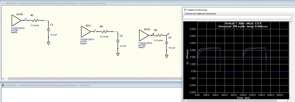
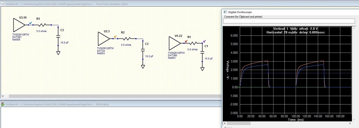
    I simulated the IBIS model here as attached. The A to B0 and the A to B1 shows capacitive loading but B to A didn't show similar behavior.
    The snapshot shows the simulation done at 5 ohm R and 10pF loading, 1Mhz frequency.
  • attachment below shows the same IO behaviour for 10Mhz frequency , note the loading effect on the IO channels which cannot reach the full 3.3V range.

  • Dear Shreyas

    thank you , it is clear now for me !! but where does this 5 OHM 10PF come from ? you see that in my simulation , there is no PCB , no components , only TXS02612 , even more , the soldered line is short .

    in my simulation setup , the B0 is floating .

    thank you very much ~~
  • Dear Wang If you look in the datasheet of the device, the Cio for the A port is 7.5pf max and 10pF max for the B port.
    The wires will also add distributed cap loading however short it is.

  • Hi ShreyasRa,

    I am FAE supporting this customer.

    For this case, if 10M is required, is it possible that we can add another high speed level shift after the TX02612 to re-sharp the waveform, if the new level shift can have wide input high level/ low level range?

    If possible, could you please recommend a device for this case?

    Best Regards

    Charles Zhang