This thread has been locked.

If you have a related question, please click the "Ask a related question" button in the top right corner. The newly created question will be automatically linked to this question.

TXB0108: TXB0108 Buffer IC working Independently but not with other cards

Part Number: TXB0108

Hi

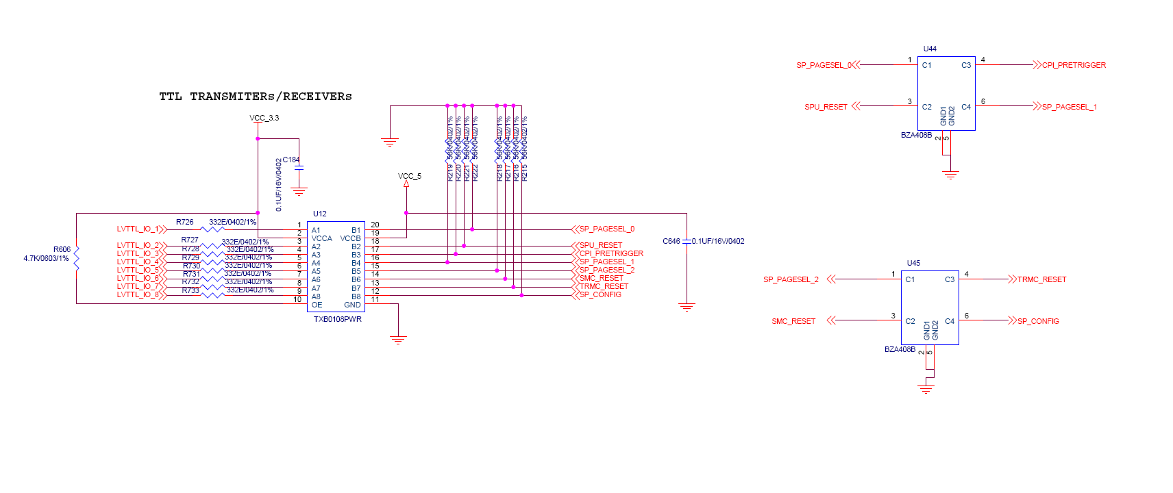
We are using TXB0108 in one of our project.

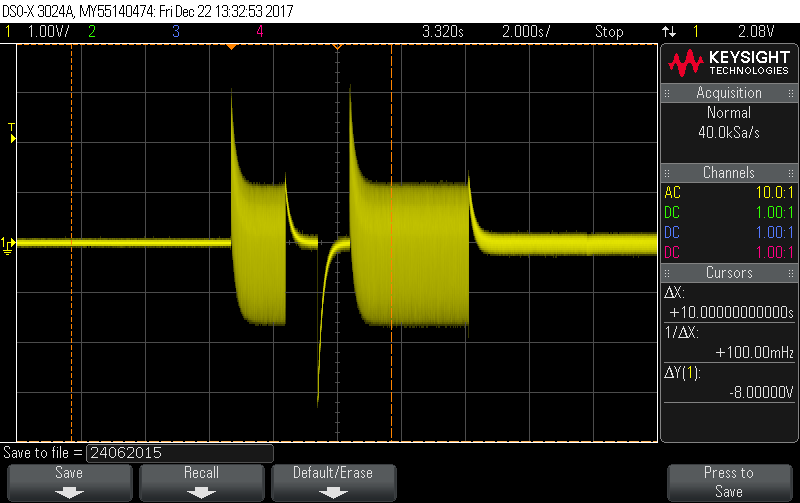
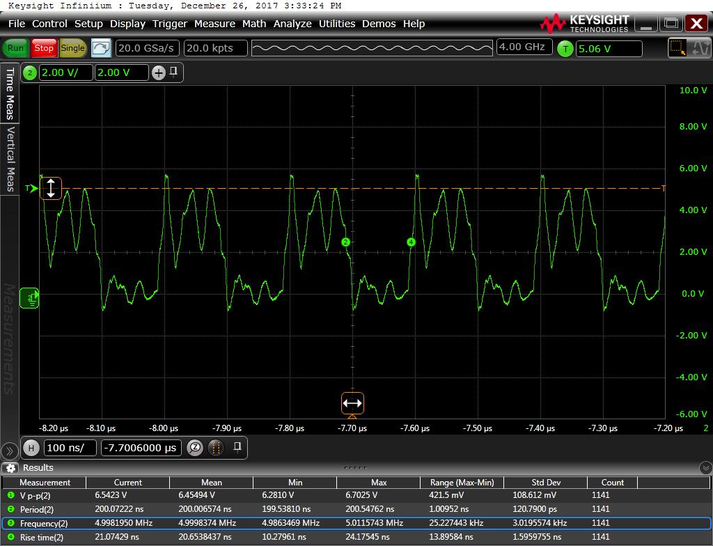
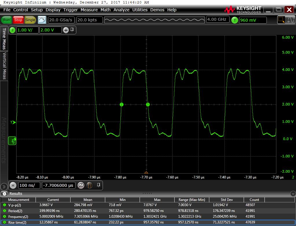
When tested independently on oscilloscope and when loopbacked with same buffer other signals, the waveform transactions are ok.

But when card is connected in a System with other cards, where signal from TXB0108 are going out to other card then there is unwanted oscillations on the signal.

What could be the issue?

Pls check snapshots and Buffer circuit.

Need to check this closely as our  many boards are using this buffer.

Regards

  • TXB Buffer pulldowns are not mounted at present.

  • Hi Amit,
    It's likely that the capacitance between boards is too high for the TXB to drive. It is not designed to drive large cpaacitive loads.
  • Yes I checked in datasheets it is 70pF capacitor maximum what it supports.

    But now since the board is ready we need some work around to proceed further.

    we have one pull down and one schottkey  diode in path.

    Kindly suggest some thing by which the required current can be boosted.

    I have though off TXS series of ICs.  As these ICs do not have internal series 4K resistor  in path, 

    If I increase the current drive from FPGA to maximum then will it help to solve this issue.

    Kindly comment....

  • I have thought of
  • Hello,
    Our response will be delayed due to the holidays.
  • Hi,

    Can you suggest proper Thevenin Termination so that it can provide the required current to drive the load capacitance.

    I Calculated and tried R1 = 76E and R2 = 150E but waveform was not proper.

    I tried with different series termination values and found that resistor around 300E gives better shape of the waveform.

    Can you suggest proper Thevenin Termination to be used for this case.

  • Hi Amit,
    I'm afraid that all auto-bidirectional voltage translators are sensitive to capacitive loads. The only way I know to send data between boards with a backplane is to use a transceiver (direction controlled) or buffer (unidirectional).

    Adding resistors to the output of the TXB translator will not improve the situation.

    The TXS translators have internal pull-up resistors and are essentially open-drain outputs -- ie pull-down resistors on the output would not work correclty, and the device adds no drive strength.
  • Hi Emrys Maier,

    I know TXB/TXS buffers are not meant for backplane driving. We are going to change it in 2nd spin of board with proper direction buffer with high current capability.

    As this is a prototype board we want to show demo to our customers with present TXB/TXS buffer in the circuit.

    And that's why looking for possible work around.

    As this is Auto Bidirectional buffer, Can we add a very low cut-in voltage Schottky Diode in series with buffer output so that it will force to work in one direction.

    Well I want to simulate all these scenarios but buffer spice model is not available.

    Can you share TXB0108 and TXS0108 SPICE models.

    For you reference I am adding a waveform snapshot without series termination and with series termination.

    Kindly comment.

  • I understand TXB /TXS buffers have low driving capability.
    But as I know parallel or thevenin terminations are used at the output to increase the driver capability.
    Pls put some efforts on simulation to find out the actual effect of termination.
  • Hi Amit,
    "But as I know parallel or thevenin terminations are used at the output to increase the driver capability."
    -- Can you tell me your source of this information? Were they talking about CMOS logic circuits?
    A thevenin termination (in an RF transmission line, not a logic circuit) is used to achieve a maximum power transfer/minimum reflections, ensuring that 50% of power is lost in the drive/line and 50% is delivered to the load (note that a perfect match produces a voltage divider with output voltage Vo = Vin*R/(R+R) = Vin/2).

    In a logic circuit, we want to deliver maximum voltage - ie get as close to Vcco as we can on the distant end. It's generally a very bad idea to cut the voltage in half since most CMOS inputs will have issues with a Vcc/2 signal into them (oscillations, shoot-through current).

    -----

    Also, I can't really replicate your setup from the vague information above.

    Can you share the schematic for your test along with measurement points for the above scope shots? What is connected at each end of the translator? What is different in each shot (precisely)?

    Additionally, what is the parasitic capacitive load on the output of the TXB/TXS translator? Even an estimate would be helpful, or a measurement of how long/wide the traces are and how many connectors are in the signal path.

    You mentioned a "pull down and Schottky diode" in the signal path -- what are the values of these? Hopefully your schematic answers my next question of where did you put them.

    I'm happy to try to help, but I can only help when you give me enough information.
  • I will update you...