This thread has been locked.

If you have a related question, please click the "Ask a related question" button in the top right corner. The newly created question will be automatically linked to this question.

LSF0102: Vref B makes the currents flow into the Vref A power supply

Part Number: LSF0102
Other Parts Discussed in Thread: TPS62743, CC1310, , TXS0102, ATL431

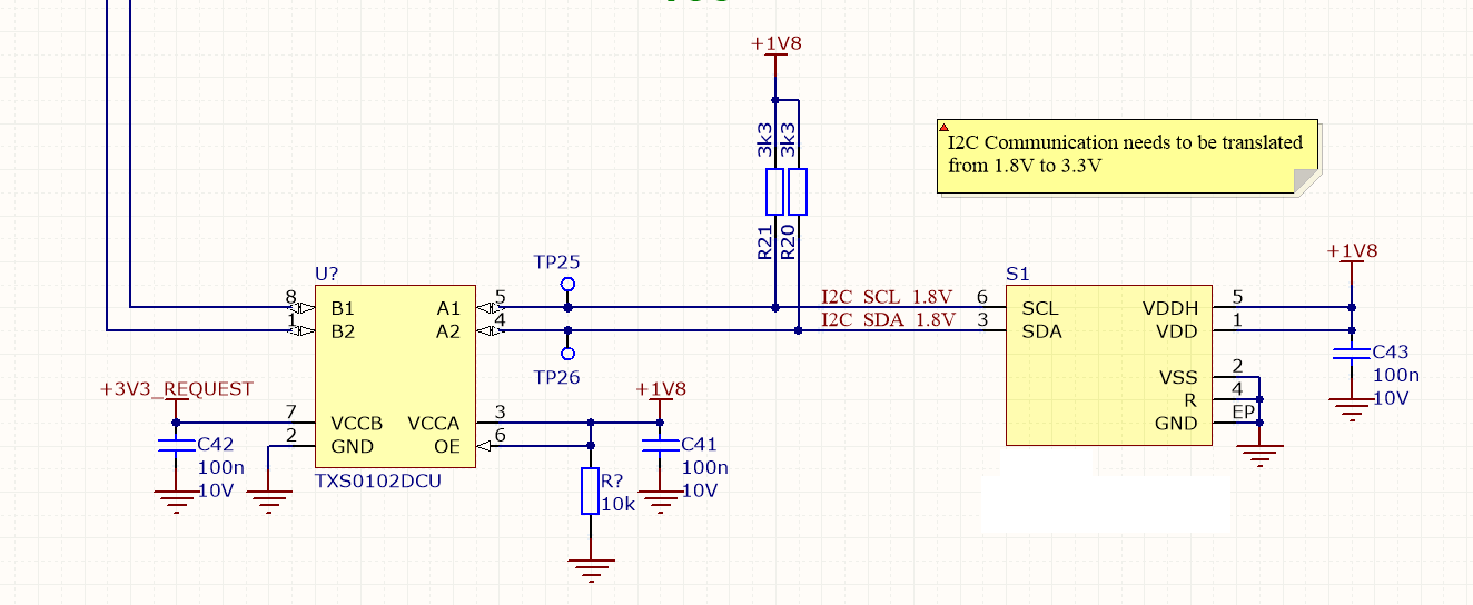
Hello, we are using level translator LSF0102 for i2c from 3.3V (master) to 1.8V (slave). Schematcis bellow, we are using TPS62743 for 1.8V power supply but we are having problem with current flows into from 3.3V to 1.8V and after turn on 2.4V is measured on output of TPS62743. If LSF0102 is unassembled output voltage on TPS62743 is correct. If we use external 1.8V power from linear power source it will handle maitains 1.8V. LSF0102 side B is controled by CC1310 on 3.3V power supply. What should we do to make this setup operationable? Best regards! 

  • Hi Filip,

    I believe that the TPS device requires some loading(current draw) to maintain the regulated output at 1.8V. The setup for LSF requires that the 1.8V has some sink capability to sink the current through the 3.3V and 200k resistor.
    could you possibly switch to TXS0102? this can get rid of your external resistors on input and output ports since TXS have internal 10k resistors.
  • Hi,

    thank you for your reply. If i understand correctly TXS0102 will help only with internal pull-up resisotrs. I need to recommend something which will help with 1.8V power supply is there some another switching regulator which can handle this LSF setup? I tried to add some load resistor to output of 1.8V switching and it helped but we need to minimize power consumption so it will have always low current load. Any other suggestion?
  • What was the load resistor you put at the output of the LDO?
    what is the minimum current required for LDO to maintain the operation?
  • Hi, 

    you mean switching regulator, i put 2k2 resistor on the output. BUT if i unassemble LSF0102 output voltage of TPS62743 is correct without load resistor! So it looks like that minimum current is not the main problem. Any other suggestion?

    Thanks,

    Filip

  • The TPS62743 has no required minimum load. If leakage tries to pull up the output voltage, it will allow this and not sink the voltage. This would be inefficient, whereas this device is designed for best efficiency.
  • Is there any other switching regulator which can handle this application?

    Thank you,
    Filip
  • Filip,

    You could try replacing the 2.2K with 450k resistor. This will hopefully help VrefA to sink current as well as maintain the loading on the regulator to maintain the output voltage.
    replacing the LDO with shunt reference device like the ATL431 could work as well which requires some current to be sunk into it to maintain the rated voltage.
  • 450k resistor could solve my problem but it will add 4uA additional current consumption, in my case every single 1 uA is critical. However ATL431 cant be used because of that i need to load TPS62743 with 2mA current consumption in periodical way (once per some time). So my 1.8V source needs to handle both cases, low and high power consumption. I am really struggling with that.

    Thank you,
    Filip
  • There is always current tradeoff in the level translation implementation.
    Sorry, if TXS0102 cannot be used in place of LSF0102, i am not an expert on the switching regulator to be used in your application. I would suggest to contact the switching regulator forum for suggestions of low power regulators.
  • If you want the DC/DC to sink the voltage, it must sink this energy to GND. This is inefficient.

    The TPS62231 operated in forced PWM mode can sink the higher output voltage.
  • We can consider use of TXS0102 but i am not sure that will solve the problem. I'll try to create topic on regulators forum thank you.

    Filip

  • good luck, please let me know how you proceed on this.
  • Let's keep the discussion on this thread, so that all are aware of the solution.

    How much current does the regulator need to sink?

    As noted before, sinking any current (to GND) is intrinsically not efficient.
  • Hi Filip,

    I read through this post and wanted to give you some additional information.

    The LSF0102 is a purely passive translator - that means that any current going into it comes back out again (with the exception of very minor leakage current), ie the current coming through the 200kohm resistor is going to go through the device and have to sink into the +1V8 supply -- something that most supplies don't really like to do. In most systems, the lower supply is being used for many things, so it's not a problem as the current can sink into any of those paths, but in yours it seems that there's nowhere else for it to go. You can see exactly how this works in our short video "Understanding the Bias Circuit for the LSF Family"

    The TXS0102 operates differently and will not produce this current into your 1.8V supply -- actually, it will sink current from the supply and should resolve this issue entirely. With the added benefit of internal pull-up resistors, it seems like a win-win situation for your design, saving board space and resolving the issue.

  • Hi, 

    thank you for your suggestion, ill try to replace LSF0102 by TXS0102 on next revision of our device and then ill write if it helped.

    Thank you for explanation!

    Have a nice day,

    Filip

  • Hi,

    I am wondering about TXS0102 enable, ill try to describe. On B-side i have 3.3V on A-side i have 1.8V  (master is 3.3V). Both voltages are switched at the same time by microcontroler (EN signal), what should i use for enable device? EN signal from microcontroler, 1.8V or 3.3V? In DS is written this:

    "To ensure the high-impedance state of the outputs during power up or power down, the OE input pin must be tied to GND through a pulldown resistor and must not be enabled until VCCA and VCCB are fully ramped and stable."

    When i use EN from microcontroller it will be always sooner than 1.8V from switching regulator and this condition will not be met. Same cas for 3.3V and if i use 1.8V for OE it will be powered at the same time as A-side and that is not good too but it looks like best option. Yes i could connect OE to microcontroller but i have almost no remaining GPIO. Another thing is that  in evaluation board on TI.COM can be found OE driven through 10k resistor to same voltage as B-side WITHOUT ANY PULL-DOWN.

    So i'm asking, if i not guarantee LOW on OE (even if device is unpluged form both sides) will internal fets be open? Because of that i'm using it for I2C and on B-SIDE are other 3.3V devices and voltage on SCL and SDA is present.

    Another question is that if i use incorrect power sequencing will device produce on A-side voltage from the B-side? (it could damage our device on 1.8V side)

    Here is our schematics:

     And here is schemtics from evaulation board:

  • Filip,

    "EN signal from microcontroler, 1.8V or 3.3V?"
    EN signal is referenced to the Vcca voltage, so it must be tied to 1.8V.
    EN signal can be tied to Vcca as you currently have it, and this will not cause any issues. I have seen this connection on most designs since everyone have GPIO constraints.
    When EN is low ( device disabled) the IO ports are in Hi-Z and disconnected from the 10k pullup resistors.
    The current setup and power sequencing will not have any adverse effects on the device.

    Since this is a new topic, for further questions, i would request you to create another post and i will consider this thread as closed.