This thread has been locked.

If you have a related question, please click the "Ask a related question" button in the top right corner. The newly created question will be automatically linked to this question.

ISOW7841: how to design to pass the EMI test

Part Number: ISOW7841

Dears,

Our product is EV BMS mother board,use ISOW7841 isolate SPI signal.

For ISOW7841,we use 5-V input supply operation,for EMI test,we test RE in ALSE,the result is bad at 238M frequency,is about 60db,more larger than the normal value 38db.we have study the SLLA368A file,so have 3 question:

  1. If use Y2 CAP,how about the effect on 238M frequency point?Pls promote us a full part number if OK.
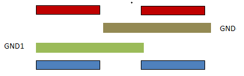
  2. If use Extending the internal reference layers creating a stitching capacitance,as below shot,how about use the two isolate GND layer,GND1 and GND2  to creat the stitching capacitance?not as the SLLA368A said use GND1 and VCC2,it will be OK?
  3. to  calculate Ci,we should consider the two GND1 and GND2's overlapping area,do we need to consider the GND1 layer or the GND2 layer themself area?

  • Hi,

    Thank you for using E2E forum and for evaluating ISOW7841. Please find below my inputs to the questions you have posted.

    1. The Y2 cap is mostly effective for the frequencies less than 200MHz. It will still have a small improvement for frequencies higher than 200MHz. Any HV Y2 SMD cap with a capacitance of >100pF should be good. It is also good of the leakage inductance of the capacitance is lower.

    2. Any power supply layer one side to any power supply layer on the other side is fine for creating the inter-layer stitching capacitor. This is primarily for the reason that, all the DC sources are considered short by AC high frequency radiations. Hence GND1 to GND2 inter-layer stitching cap is not an issue.
    Since this is for automotive application and most likely the emissions standard that you need to comply to is CISPR 25 Class 3, it is good to have an inter-layer stitching cap of at least 100pF. This cap is mostly effective for frequencies higher than 200MHz.

    3. Yes, for calculating the capacitance you will need to consider GND1-to-GND2 overlapping area only and not the overlap GND layers.

    Please do implement these recommendations and let us know the results once you test these boards. If any of the above points are not clear, please do let me know so that I can clarify it further. Thank you.


    Regards,
    Koteshwar Rao