This thread has been locked.

If you have a related question, please click the "Ask a related question" button in the top right corner. The newly created question will be automatically linked to this question.

ISOW7841: ISOW7841 EMI issue

Part Number: ISOW7841
Other Parts Discussed in Thread: TIDA-00893

Hi Sir,

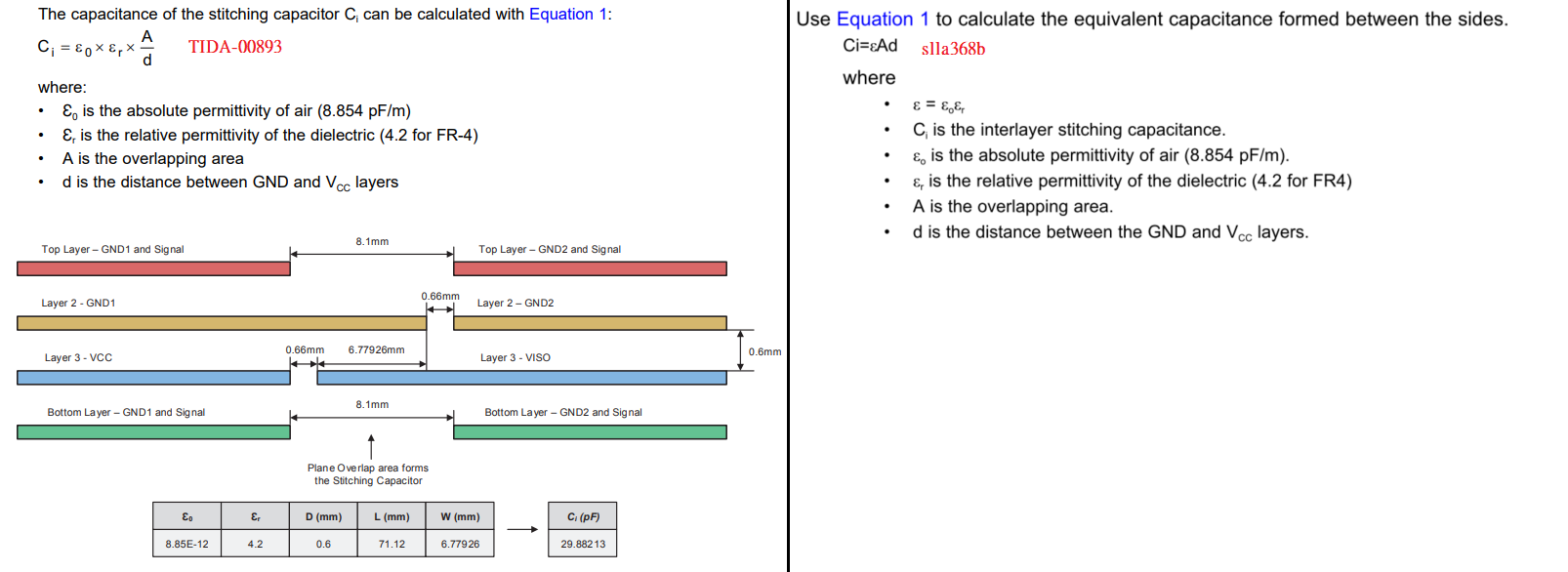
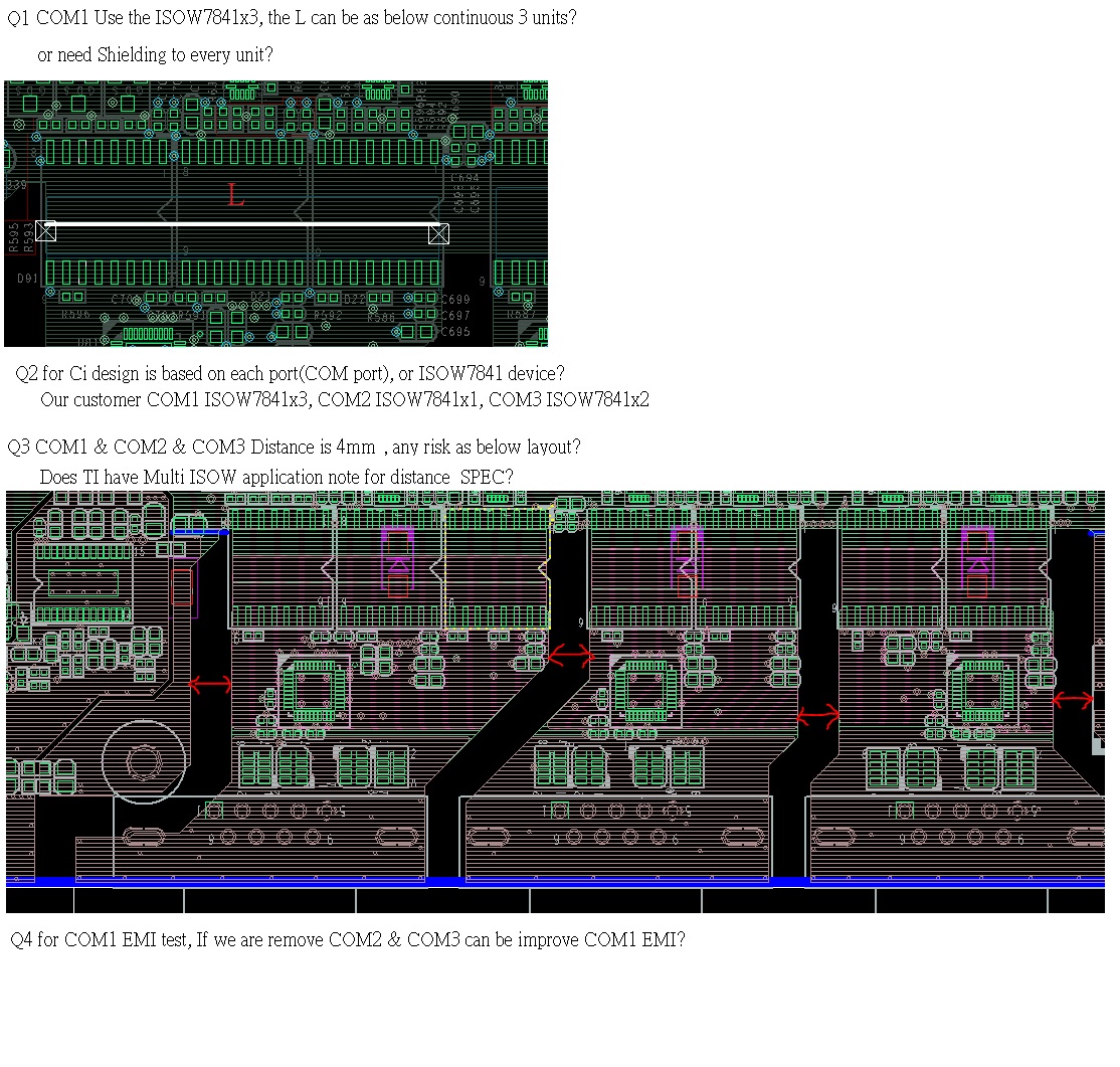
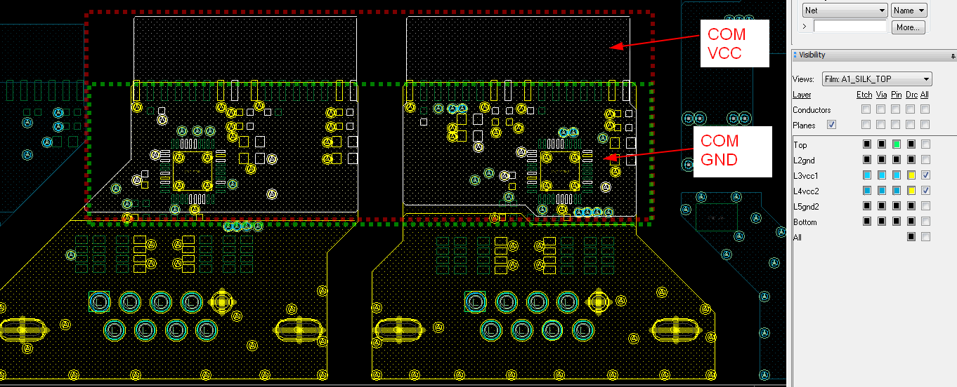
Our customer used the ISOW7841, But EMI report Fail.

Could you please support for Review Layout?

or based on EMI report Could you please provide the suggest for me?

Hugo

108-01-31-M1923.pdf

  • Hi Hugo,

    ISOW7841 emissions are affected by factors such as layout and operating conditions. Can you include more detail of the setup? For example, what are the Vcc and Viso values? What is the load on Viso?

    PCB layout can greatly improve performance if designed using the considerations in this application report. Please encourage our customer to review their board layout to ensure it includes a stitching capacitor and y-capacitor as mentioned in the linked app report. Additional comments regarding common mode chokes are provided in this E2E post.

    Is this helpful? Please let me know!


    Thank you for posting on E2E,

    Manuel Chavez

  • Hi Sir,

    Thank for your response,
    VCC=5V & VIOS=5V SEL=VIOS
    VISO Load need check with customer.

    we are see the Application have RF on Figure 5.
    What's the Value for Suggest?

    Hugo
  • 1) Use CM choke in input and output with impedance > 1K  for Freq. < 100 MHz in RE test 

    2) Make Stitching capacitance as per application note from TI. for Freq. > 200 MHz in RE test

    3) After these changes best of luck.

  • Hi Harish,
    Thank you for helping with your input to reduce radiated emissions. Appreciate it.

    Hi Hugo,
    Sorry to hear that customer is facing radiated emissions issue.

    I see that you have shared two sets of emissions plots - one with EUT only and the other with all interfaces like USB, LAN, RS-232, etc. Will you be able to share us what exactly does customer mean by when interfaces like USB, LAN, RS-232 and others are added? Does this mean they are adding one communication board with all the interfaces listed?

    I see that the radiations are much higher when all the interfaces are added and exceeds as high as 20dB. Most of the radiation is seen for frequencies >200MHz, this explains that the test setup doesn't have too many unnecessary cables. To reduce radiated emissions for frequencies >200MHz, it is recommend to implement a stitching capacitor using internal PCB layers and achieving a value of >50pF. Please refer to the app note SLLA368b section 4 for more information related to implementing stitching capacitor. Once the stitching capacitor is implemented, you should see good results. Thanks.


    Regards,
    Koteshwar Rao
  • Hi Sir,

    Thank for your explanation.

    our customer tell me , VISO load <20mA(5V),

    But for test COM port only have cable, the device not power on EMI is over spec.

    The USB/LAN/RS232/DP connector is on same PCB, if note "EUT only" is not connect to any deice(USB/LAN/RS232/DP).

    They are try to COM port metal case to GND, EMI 400~500MHz base will be reduce.

    They are doubt this issue is fromCOM port ground.

    we have some question, could you please share your suggest for me? 

    Q1, we are see the TIDA-00893 & slla368b have different equation for Ci. we can ref which one?

    Q2, we are try to calculate Ci Value as below, need change to >50pF? I see the D(mm) only 0.1 any risk? 

    Q3, the slla368b Figure 5(RF+L1) & Figure13(Common-Mode Chokes) to reduce emissions, Is this only one on PCB or both use?

    Hugo

      K=Er(4.2 for FR4) Eo(F/m) D(mm) L(mm) W(mm) C(pf)  
    PCB 4.2 8.854E-12 0.6 77.3 6.28 3.00868E-11 TI ref design
    PCB 4.2 8.854E-12 0.1 30.8 2.62 3.00083E-11 Customer COM1
    PCB 4.2 8.854E-12 0.1 20.16 4.01 3.00624E-11 Customer COM2

  • Hi Hugo,

    Thank you for sharing additional information.

    You are right, the COM port by itself shouldn't be an issue but when they are connected to ISOW the radiations from ISOW get larger due to connections on COM port. I also understand that connecting the components on COM port should be a necessary for the end-equipment and can't be eliminated.
    Implementing the stitching capacitor that is formed using PCB layers should enable the PCB meet the emissions requirement even with the connections on COM port.

    Regarding your questions,

    A1. Sorry for the confusion, recently the App Note SLLA368A was updated to SLLA368B and during this update seems like the formatting in the equation got corrupted and eliminated the '/' symbol between 'A' & 'd' from the equation. Please use the equation in TIDA-00893 User Guide.

    A2. It would be upto customer to keep the suitable value for D based on how much of the spacing between layers is acceptable to their applications. I will be able to comment better if you can share us the customer isolation requirements.
    Please note that, customer can also increase A (area) to achieve higher Ci value though it will take up more PCB space.

    A3. Regarding Figure 5 and Figure 13, did you mean to ask if customer needs both the ferrite bead and common-mode choke (CMC)? No, customer doesn't need both. Only the CMC should be sufficient.
    Looking at customer emissions test results, it doesn't look like customer would need CMC. Using the stitching capacitor with >50pF value should help reduce emissions significantly.

    Please do suggest customer to implement the suggestions and let us know if they have any questions, thank you.


    Regards,
    Koteshwar Rao
  • Hi Sir,

    Thanks for your support,
    We will check with customer.

    Hugo.
  • Hi Sir,

    we have 4 question from customer, 

    could you please share your suggest for me?

    Hugo

  • Hi Hugo,

    I will be happy to provide answers to your questions, please find below my inputs. Thanks.

    A1. If all the three devices share input and output GNDs then L can be continuous the way you have shown in the picture and there is no need to split it.

    A2. Ci design is not based on the each COM port, it is for the device ISOW78xx. I understand the number of devices for each COM port are different, it is not necessary to have proportionally increasing cap. A safe value for stitching cap is 50pF, if you have at least 50pF for each stitching cap then the board should produce good results. If possible to achieve higher values of cap, please feel free to implement higher values as well but nothing less than 50pF.

    A3. It looks like all the COM ports are isolated from each other, if so then the spacing between them should be decided based on the isolation that customer wants to achieve between. If the COM ports only need ground loop isolation then spacing shouldn't be very critical. Either ways, if the isolation requirements are not very high then 4mm should be a decent value to start with.

    A4. Since this is a radiated emissions test, presence or absence of devices will make a difference to the overall results observed on the PCB. There won't be any impact of one device emissions on another device.


    Regards,
    Koteshwar Rao
  • Hi Sir,

    Thank you very much,

    I have one question from customer,

    If the GND & Vcc Stacking method change to Right picture.

    then effect Ci calculate or performance?

    Hugo

  • Hi Hugo,

    The two implementations that you have shown are valid and produce the same capacitance value as the overlap area (A), the spacing between layers (d) and the dielectric material are still going to be the same. It is fine to use either of the options. Thanks.


    Regards,
    Koteshwar Rao
  • Hi Sir,

    If our customer two COM Port use one common VCC  similar red area, two COM Port use one common GND similar green area to get more Ci>50pf.

    That mean no shielding between COM2 & COM3. any risk? we can do that ?

    Hugo

  • Hi Hugo,

    If customer board has common VCC & GND for two COM ports (COM2 & COM3) and decides to use a bigger common area to create >50pF then yes this should cover all the devices in COM2 & COM3 and these two ports might not need a separate individual stitching caps.
    If COM1 is not sharing VCC & GND with COM2 or COM3 then COM1 will need a separate stitching cap with value >50pF>

    Does this answer your question? Thanks.


    Regards,
    Koteshwar Rao
  • Hi Sir,

    Thanks for your grent support,

    Hugo