This thread has been locked.

If you have a related question, please click the "Ask a related question" button in the top right corner. The newly created question will be automatically linked to this question.

ISOW7841: data and power isolation for data acquisition with ads8668

Part Number: ISOW7841
Other Parts Discussed in Thread: ADS8668, DAC7571, CD74HC4067, TIDA-01214

 Hi

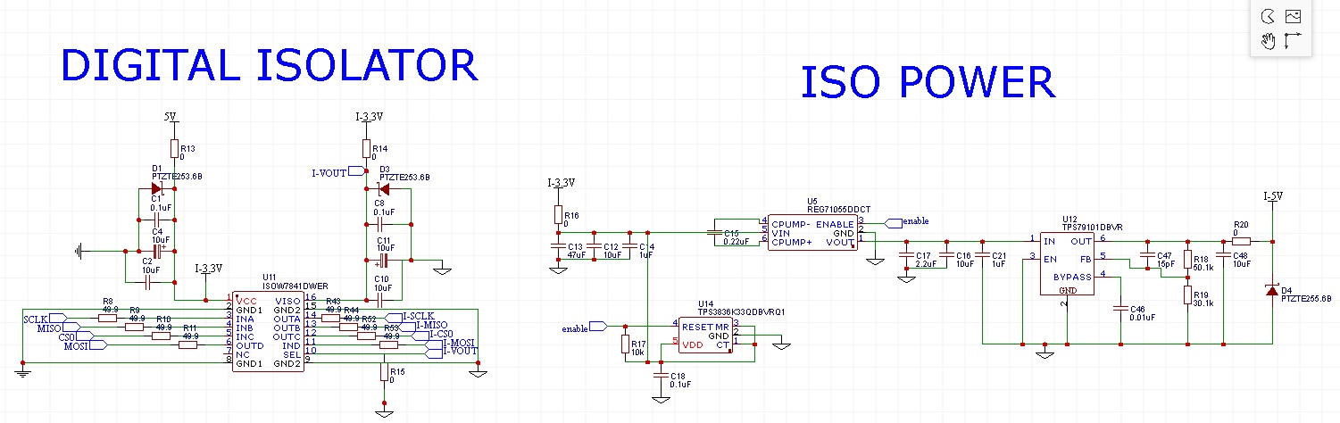
As refering to TI design TIDA 01214 i wired the data isolation as in the picture. Do you see any errors? Thanks a lot and regards

  • Hi Pierluigi,
    I do not see any glaring issues at first glace, but please allow me to review this with the team on Monday. What is the zener voltage of the diodes?
    Best regards,
    Dan
  • Hi Dan,
    the diodes close to isow7841 should be 3.9V, D4 on the bottom 5.6V. In the software i used the right parts weren't available (diodes).
    Hope you guys can help me with pcb layout as well. Thanks a lot for your fast answer.
    Best regards,
    Pier
  • Hi Pier,

    I have a few notes after reviewing this with the team:

    1. C1 and C8 should be closes to the supply pins in the layout. The 10uF caps should be placed close to the device as well. They should be placed on the same plane as the device. 
    2. Zener diodes look fine
    3. R12 is not needed. NC can be left floating. But it can be left as is in your schematic and will not cause an issue
    4. Current limiting resistors R8-R11 are fine. They can be implemented on side 2 of the isolator if you wish. 
    5. Please refer to Section 11 of the ISOW datasheet titled "Power Supply Recommendations" and follow the recommendations accordingly. 

    We would be happy to review the layout as well. You can either reply to this thread with the layout or start a new one. 

    Please let me know if you have any questions. 

    Best regards, 

    Dan

  • Ok!

    I will put those resistors and leave NC floating.

    On the power side we have two regulators at 1A , a 3.3V and a 5V (this one used only for 2 leds at present), i think it is going to be ok right?

    I would like to ask if you can give me some hints, or documentation, on how to lay down digital and analog grounds on pcb. I will start to work at the pcb as i get an ok on the ADC wirings.

    Thanks a lot Dan,

    have a nice day you and all the team!

    Best regards

  • Hi Pier,

    Thank you for your good wishes! Please allow me to respond since Dan is on business travel and his next response might be delayed.

    Is the ISOW7841 connected on the same regulated output as the LEDs? 1A regulators should be plenty to power the ISOW7841 and both LEDs, but can you share the LED part numbers to confirm?

    Regarding ground planes, it is not always beneficial to separate analog and digital grounds since this can concentrate charge in areas of the ground plane. Attached are some starting guides for PCB and mixed signal grounding. Which ADC is used in this project?


    Thank you for your time,
    Manuel Chavez

    Grounding in Mixed Signal Systems Part 1 - slyt499.pdf

    PCB Layout Tips for High Resolution - slyp167.pdf

  • Hi Manuel,

    So, we have a 1A 3.3 V which is feeding on the main board (not the one with isow7841) many potentiometers ,  switches and 9 leds, at present i used this supply for isow7841. maybe this is not good, right?

    Then we have a 1A 5V which is meant to feed on the main board  teensy 3.6 (80-100 ma) .and 2 leds that are going to be PWMed. So, those 2 LED could be powered by teensy itself and that's it.

    Maybe is better this 5V supply to derive I-3.3V and I-5V?

    The ADC used is ADS8668 (2 in daisy) 

    On the ground side,  the ads8668 ref. manual strongly reccomends separating grounds, i guess in not an easy task at all...

    i will have a look at the links, thanks a lot!!

    Pier

  • Hi Pier,

    Hopefully the links above have provided useful considerations for this design and not been confusing! Thank you for your patience while I consulted with experts regarding this post.

    At Vcc = 3.3V and Viso = 3.3V operation, the ISOW7841 could draw a maximum current of about 200mA from the regulator. This is an extreme value and may never be seen in operation, but the ISOW could be a significant load to the 3.3V regulator if the LEDs, switches, and potentiometers together draw >800mA. Checking their Icc currents on respective datasheets will clear this concern.

    If the 5V regulator has margin to power the isolator, the ISOW7841 could provide an isolated 5V supply that has a 3.3V LDO to realize both isolated rails. What are the isolated load requirements?

    Regarding the ADC and grounds, it can be challenging to incorporate separate grounds in complex systems, so the ADS8668 datasheet offers a note in Section 11.1 that a single dedicated ground plane is strongly encouraged. A clean ground takes priority over separate grounds to achieve the ADCs' specified performance; please ensure that the AIN_xGNDs are between -0.3V and 0.3V. With this in mind, a single ground plane is acceptable to use.

    How is this design and project going? I look forward to your update!


    Thank you for your time,
    Manuel Chavez
  • Hi Manuel

    Thanks a lot for your time. Well, yes, links clearly did show me how master to perfection those things is really meant to be up to a research team, not to a single musician ... :-D

    Really interesting readings, anyway ok, i will go for the single ground , but, as we get GND from the main board where we have pots, switches, leds and opamps, regulators

    in my low understanding i'm guessing that that ground would be quite "dirty". Is so? and if so could there be a way to "clean" it before getting to the ADCs board? 

    The ADCs board is allocating also a DAC7571, 4 CD74HC4067 and Teensy 3.6 (all these need 5V and together should be under 200mA)

    Should I include anything else from above in the iso power? (the DAC?)

    The isolated load requirements should be the 2 ads8668.(they should not be over 60mA for AVDD and 1mA for DVDD)

    I guess the 5V 1A supply is the best option. I would like to add that the main power supply is a 12V 1.2A, that should be ok right?

    Let me know what you think 

    Project is really freaking me out! :-D But you guys at TI are fantastic and hope to get at the start of the wiring tunnel soon...

    Thanks again Manuel

  • Hi Pier,

    You're welcome! The single ground cleanliness can be preserved by physically locating switches, pots, op amp, and regulators away from the ADC and routing digital signal lines away from analog lines. Any analog lines that run parallel next to each other may experience crosstalk.

    "Cleaning" the ground shouldn't be needed if you keep the above considerations in mind :) Are any inductive loads connected to this ground?

    There is margin to include the DAC on the isolated power supply if it's necessary. Would you like to share a system block diagram? I can reach out via email or Message on E2E for this.

    The 12V main power supply is okay for the load requirements included above, but it is worth confirming the LEDs, switches, pots, and op-amps current levels.


    We're glad to help! Best wishes on this project.


    Have a great weekend,
    Manuel Chavez
  • Hi Manuel and all team. 

    Happy easter, and, please have a look at the img, for a confirmation.

    I fed 5V to the circuit as we said, added the 49ohms resistors. i had to stop few days cos too much work. hope this is finally right, Kind regards

  • Also, i would need a bom list for those caps and res here. Could you help me with that? i couldn't find a bom in the evm files
    Regards
  • Hi Dan, i came out with this pcb design, hope is not too bad... 

    i did post also the latest schematic

  • Hi Pier,

    Thank you for your warm wishes! I apologize for the delayed response. Regarding the schematic posted last Sunday, please confirm whether you would like the Viso output to be 3.3V or 5V. In the 3.3V case, SEL should be grounded or left floating instead of tied to Viso. If SEL is tied to Viso the output voltage will be 5V.

    A BOM of the ISOW7841 EVM is available on page 5 of the EVM User's Guide, and a copy of the table is shown below:


    Regarding the PCB layout, please place the smallest capacitors closest to the ISOW7841, meaning C1 closest to Vcc and C8 closest to Viso, with larger capacitors following in order of value.

    Although the EVM shows three capacitors on Vcc1 and Viso of the same values, if voltage transients are expected in your system where Vcc would drop below 2.7V, an additional 100uF capacitor on Vcc (pin 1) is strongly recommended for reliable operation.

    I noticed there is a connection between Pin 1 of the ISOW7841 and R14 on the PCB. This connection is not necessary since Viso is a sourcing pin, meaning that power will flow out and if an additional supply is connected there may be damage. There is also no visible isolation between grounds in this configuration, is isolation only required on the data lines?


    Thank you for your time,
    Manuel Chavez

    PSA: Post edited to correct the placement of 100uF cap on Vcc, Pin 1, of the ISOW7841. For details, please refer to the Power Supply Recommendations section of the ISOW7841 datasheet.

  • Hi Manuel, thanks for your time
    So , not bad for a guitarist eh? ;-)

    "A BOM of the ISOW7841 EVM is available on page 5 of the EVM User's Guide, and a copy of the table is shown below:"

    Thank you, but i didn't get the design from the evm but from TIDA-01214, something missing there..
    on supply. we go for 5v

    On Grounds, Dale from ADC dep. told me to have a single ground board, considering there are many others ics, that (have separated grounds) would require a particular study, to be really useful.

    ok, i'll put the 100uF capacitor and be back to you on private

    Regards
  • Hi Pier,

    I was just discussing this thread with Manuel in the office. I just wanted to emphasize that GND1 and GND2 should not be connected and Vcc and VISO should not be connected. Shorting GND1 to GND2 will not damage the device - but will essentially mean you have no isolation. And why are you using an isolation part if you do not need isolation?

    Take a look at the ISOW7841 EVM layout:

    Notice how there is a gap between the two sides of the device. There are no traces between the two sides of the device. This is what we need to consider on your layout. There needs to be a clear boundary - free of any conductive materials (traces, other components, etc.) - between the two sides of the device to isolate one side from the other.

    Best regards,

    Dan

  • Hi Dan,
    this is really interesting. For what i could understand, using ads8668 in the perfect scenario would mean that grounds are separated, at half level of the ADC chips ( as shown in ADS8668 datasheet at page 70) .
    I've already done that layout (with separated grounds), painful, but the ADC department told me to followe the TIDA design i mentioned and that is better to have a single ground plane for the whole board, as also written in page 69.
    In the latest layout there is only one ground, coming from the first board . is named AGND as on the other board
    I've been talking with Dale li for the setup of ADS8668. i tried to keep all other ics on bottom layer also for this reason.

    I think doing what you say is possible on the top layer, but i still don't understand how (in ads8668 datasheet) what is written in page 67 and 69-70 comes together in reality...
    Please help :-D
    Kind regards
  • Hello Pier,

    My apologies! A copy of the TI Design BOM is on the TIDA-01214 webpage in the Design files section (underneath the CAD/CAE Symbols). Here is a link.

    For 5V operation, the SEL pin connection is correct. The 100uF capacitor can also be placed near Vcc1 with the other decoupling capacitors as long as it is the furthest away from Viso pin because it is the largest.

    As Dale said, separating analog from digital grounds may be overly complex for this case, but Dan brought up a good point about using the ISOW7841 above. This digital isolator is not meant to isolate analog from digital grounds - it is meant to isolate mixed-domain grounds from each other, protecting them from ground loops, transients, and other dangerous potential differences. When using the ISOW7841, please ensure there are no connections between the left and right sides. The grounds can be shared, but this defeats the purpose of the isolator. I've attached a PDF of TIDA-01214 PCB layers to demonstrate the separation of both sides.

    Please let us know if this is helpful!


    Thank you for your time,
    Manuel Chavez

    PSA: Post edited to correct the placement of 100uF cap on Vcc, Pin 1, of the ISOW7841. For details, please refer to the Power Supply Recommendations section of the ISOW7841 datasheet.

    TIDA-01214_DAISYE1_PCBlayers.PDF

  • Thanks a lot for you attention and time guys,
    The BOM will be really useful,
    on PCB design that pdf really makes sense . Problem is translating that here....
    Is that a 3 layer board right? shall i go for more layers in the pcb design? actually are 2 layers
  • Hi Pierluigi,

    I apologize for not responding sooner. The PCB in the PDF file is made up of four layers:

    1. Top signal layer
    2. Internal GNDs layer
    3. Internal power layer
    4. Bottom signal layer

    The block diagram in Figure 2 of the TIDA-01214 TI Design documentation is helpful to understand the structure of this system and shown below:


    This topology shows how to isolate up to 16 parallel ADC channels using the ADC8668A and ISOW7841. If this is your requirement, the image below shows how a general PCB layout could look with the separate ground planes outlined in blue and orange. Please notice that the ISOW7841 makes connections to both ground planes separately.


    Of course, 16 isolated channels may be excessive for your system, and maybe only 8 channels need isolation while the other 8 can remain non-isolated as shown in Figure 8 of the Reference Design.

    The second ADC is optional based on your system needs; how many data channels do you need to be isolated?

    The power rails are looking better based on previous posts, but a crucial element here is to clarify and ensure is that the ground planes are separated for isolation, not ADC performance, and the proper components are placed on their respective sides of the isolation barrier (Ground 1 or Ground 2).


    The isolation team will await your response, and please let us know how we can help you successfully complete this project.


    Thank you for your patience and for posting on E2E!

    Manuel Chavez

  • Hi Manuel and everybody..

    Of course, 16 isolated channels may be excessive for your system, and maybe only 8 channels need isolation while the other 8 can remain non-isolated as shown in Figure 8 of the Reference Design.


    Actually there are 15 inputs that deserve the same treatment, so if i got it well, this is the case.

    The PCB design you link is not new to me, problem as i said is translating it here.

    Please give me some hints on the setup of the power and ground layers to be done

    Actually expander on the left , the 2 mux on bottom right and teensy are placed on bottom layer, all the rest is on top layer, so i hope the placement of isow7841, and the related components looks right.

  • I add some useful things. power (5V and 3.3V) and ground are on the upper left of the 20 pin connector.
    the 20 pin connector also brings in 15 signals from switches. i forgot to mention the DAC7571 actually on top layer.
    Please don't hesitate to tell me whatever you feel is needed to be done
  • Hi Pierluigi, all,

    A summary of our email conversation:

    • it is okay to place components on separate layers, even on the same x, y coordinates
    • some connections previously shown cross what would be the isolation barrier, rendering the ISOW7841 useless. This can be fixed in PCB layout
    • TIDA-01214 does not need to be isolated if modified for this scenario. Isolators do improve reliability and robustness and are necessary when large ground potential differences are expected

    For the continued conversation, Pierluigi and I will work on this specific design and no further updates will be posted. Please feel free to contact me for assistance with similar questions or concerns.


    Thank you for your time,
    Manuel Chavez