This thread has been locked.

If you have a related question, please click the "Ask a related question" button in the top right corner. The newly created question will be automatically linked to this question.

Analog to Digital Ground connection

Hi TI experts,

My board uses several components that use analog ground, among them are the processor, LDO, PLL, temperature and humidity sensor and other components associated with the analog part. I cannot use the typical Starburst-type routing (although in theory option #2 is it, but in a non-standard view/placement), since the location of the components and the available space for wiring do not allow this. I also cannot use two full selected separate planes and connect them with through-hole, as this will increase the number of layers of my board, which in turn will harm the economic component. I highlight two options for myself at the moment and ask for your advice on which one is recommended from the point of view of TI for better performance of EMI/EMC?

Available options:

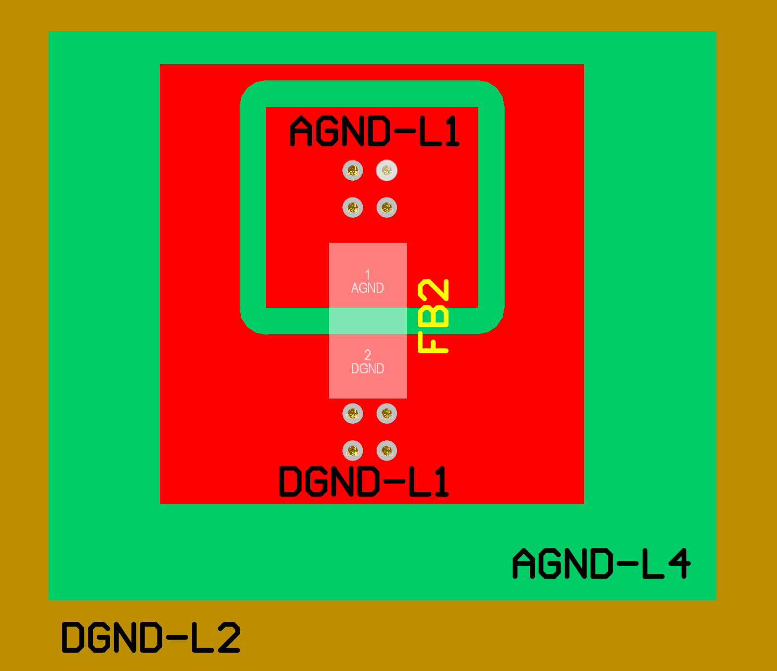
1. Use a ferrite bead between AGND and DGND polygons. (agnd-dgnd-fb.png)

Description:

AGND-L1 is used only for AGND-L4 (AGND main plane - components are connected via vias) connection with DGND-L2 (DGND main plane)

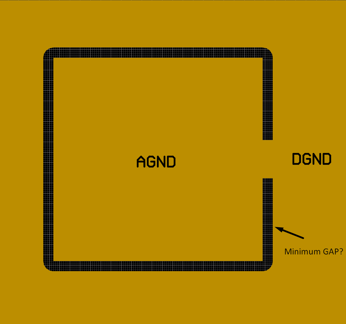
2. Make an AGND polygon with insulation (on the main DGND ground plane) and connect it to the main polygon with a small section of copper. (agnd-dgnd.png)

Description:

Both AGND and DGND polygons are on the same inner layer L2. AGND is placed in the center of this layer, surrounded by DGND, due to the fact that the element can not be placed differently due to the overall layout of the board.

Additional Information:

The board uses one input operating voltage coming from the power supply in the form of VCC (12V) and GND, subsequently located on layers L2 (GND) and L7 (VCC).

Question about options:

a. Which option is better in terms of EMI / EMC?

b. Does AVCC require the installation of a ferrite bead at the input, when connected to a VCC digital power supply?

c. Should analog signals pass exclusively over analog ground? Does this apply only to signals or to analog power supply as well? Or is the only requirement that there should be no discontinuities in the plane over which they pass?

d. In the case of option #1, the installation of two components is required? Input FB1 and output FB2? Or is one FB2 (output filter) enough to filter GND return currents?

  • FB1 - at the power input VCC => AVCC
  • FB2 - at the AGND => DGND

e. What should be the size of the minimum gap between AGND and DGND? (for voltage below 12V)

f. Is it necessary to connect capacitors providing capacitance / bypass for AVCC to AGND or can they be connected to DGND? Does it matter?

g. Does option #2 apply to ground current loops? Explanation: the digital ground surrounds the analog, will it affect it with sufficient isolation?

h. What affects each other more? (in terms of EMI) Digital signals to analog or analog to digital?

i. Can planes overlap each other if analog and digital ground are placed on different layers? What is it fraught with?

  • Hi Evgeniy,

    The DGND and AGND separation and connections related questions are best answered by the ADC team, I am notifying the relevant team to help you with correct answer. Thanks.


    Regards,
    Koteshwar Rao
  • Hi Evgeniy,

    Meanwhlie, I noticed that you had referenced this post in processors forum and did hear back them. Hopefully you had some of your questions answered. Meanwhile, please do go through the below two part article that talks about grounding in mixed-signal systems. Thanks.

    https://e2e.ti.com/support/processors/f/791/t/792937

    www.ti.com/lit/an/slyt499/slyt499.pdf
    www.ti.com/lit/an/slyt512/slyt512.pdf


    Regards,
    Koteshwar Rao

  • Hi Koteshwar,
    Thanks for your help,

    I studied the documents you submitted, but they do not provide answers to most of the questions I have asked. In connection with the additional study of the document:
    www.ti.com/.../slyt512.pdf

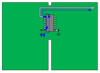
    a.a. On "Figure 3. Ground-plane bridge for traces" in the place of the bridge (red rectangle) what type of signals pass? Analog or digital? Or both (Mixed)?

    According to

    "Figure 3. Grounding data converters with high internal digital currents"
    a.b. Should the analog part of the ground and digital, have separate connections to the power source?

  • Hello,

    Here is a link to an FAQ thread that we have on this topic. It provides very high level guidance compared to the more specific questions you're asking, but shows our preferred recommendations. You will need to tailor these recommendations to your specific application.

    e2e.ti.com/.../755516
  • 1. Please give your comment on option # 2. Will the earth around (DGND) influence the analog one? Will there be a current loop? Or electromagnetic exposure?
    2. Nowhere among the documents submitted by you is it said about the connection of a divided land plot on 1 inner layer. Should analog and digital ground be connected separately to a power source? (question a.b.) (ok2.png)

  • 1.) In terms of EMC it's going to be better to have a solid continuous ground plane. Currents will return to their sources through the paths of least resistance so if you do a good job with placement of your analog and digital components you'll likely find it possible to keep the two currents from directly overlapping with each other which could result in some of the undesirable coupling you're trying to avoid.

    2.) The two grounds need to be shorted together, at bare minimum directly below the IC, preferably through a larger connection like the one shown in the image you copied.