This thread has been locked.

If you have a related question, please click the "Ask a related question" button in the top right corner. The newly created question will be automatically linked to this question.

SN6501: Behaviour of SN6501 in case of overvoltage -> Internal Diodes, Latch Up?

Part Number: SN6501
Other Parts Discussed in Thread: SN6505B

Hello,

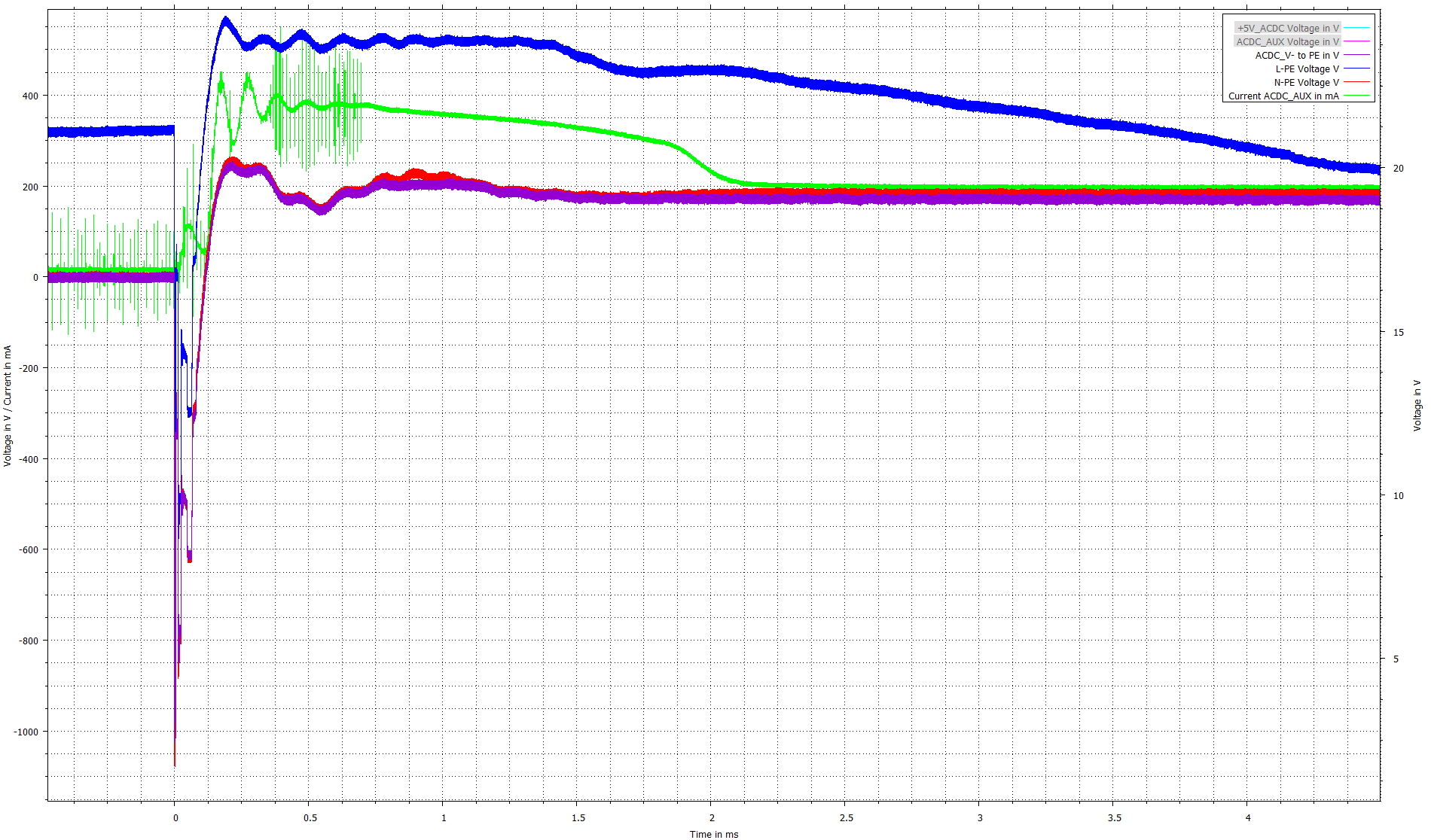
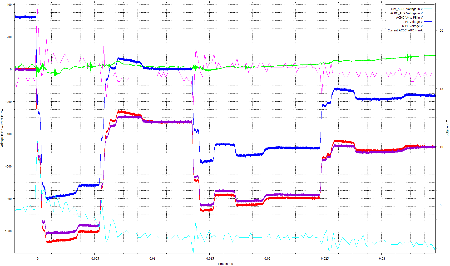
I'm currently having a issue with a circuit in which a SN6501 is used. It looks like that surge impulses on the AC-line can pass through the AC-filter, ACDC-converter, +5 V linear regulator and the SN6501 connected to this. At the moment of the surge, a extremely short voltage peak (maximum 1 us) of ~ 6 V can be seen on the 5 V rail. This is also the absolut maximum voltage rating of the SN6501. After this peak, it somehow increases its current consumption to ~ 400 mA and will fail, propably because of overheating.

As we are still looking for the root cause, I'm thinking about the internal components of the SN6501. Are there any clamping diodes that will get conductive in case of supply voltages above 5 V? Or could this device be affected by a latch-up effect due to this spike?

Thanks in advance,
Christian

  • Hi Christian,

    Thank you for posting to E2E! A Zener diode with 5.5V or 6V Zener voltage like 1SMB5919BT3G or 1SMB5920BT3G can be used to protect the SN6501 from voltages above the 5V rail.

    To fully analyze the device's behavior, can you share oscilloscope images of the waveform? As well as oscilloscope waveforms of the D1/D2 pins during this surge impulse?


    Respectfully,
    Manuel Chavez

  • Hi Manuel,

    I already tried to use a 5 V TVS diode to clamp the voltage, unfortunatelly with no effect. I can provide scope images, but until now I did not measure the D1/D2 pins.

    I'm currently thinking, that this might happen due to a ground shift and latch-up of the internal FETs in the SN6501. Could you therefore please provide information about the internals like if this is even possible on this device and whether or not there is a clamping diode or similar inside the device?

    Best regards,
    Christian

  • Hi Christian,

    Can you please share a part number of the TVS diode used? Additionally, details of the time it takes the SN6501 to recover from this condition (or if a power cycle is required) will be helpful along with the transformer's part number.

    Please allow me 1 - 2 days to confirm the device internals with you. In the meantime, a quick experiment to isolate the root cause is to disconnect D1 and D2 from the transformer and to 50Ω pull-up resistors as shown below:


    Thank you,
    Manuel Chavez

  • Hi Manuel,

    I used a PPSLC 05 C-LF-T7, not the best part for this, but the only I had right here for testing. The transformer is a Würth 750313734

    There are two possible things that happen, when the SN6501 is in this condition.

    1) If you recognize the SN6501 fault state and disconnect the power supply within ~ 1 second, the SN6501 works fine after this power cycle
    2) If you do not recognize the SN6501 fault state, the SN6501 will break and kill it's supply circuit as well. In this fault condition the SN6501 drains ~400 mA for ~2 ms and after that 200 mA more or less continuous, even after a power cycle. If you keep it running for ~2 s it's supply circuit breaks as well as this is only designed for ~20 mA

    I can provide you two scope images. First is a overview of the behaviour at a surge impulse at t = 0 and after that a detail. Notice the drop of the 5 V voltage in cyan on the detail image right after the surge impuls

    Blue = Voltage L to PE
    Red = Voltage N to PE
    Green = Current of the circuit which is only a MIC5235 that provides 5 V to the SN6501
    Magenta = Input Voltage of MIC5235
    Cyan = Output Voltage of MIC5235 = Input voltage of SN6501

  • Hi Christian,

    Thank you for including these waveforms. It appears the input voltage the SN6501 rises to >10V. There is no clamping mechanism in the device, and normally a latch condition is not expected. It's possible however that this overvoltage affects an internal ESD cell by exceeding the reverse bias rating at its peak (>6V is the absolute maximum rating for Vcc), creating a short circuit path internally that lasts even after the overvoltage. If the ESD cell conducts too much current for too long, like 200mA for 2 seconds, it would eventually be destroyed.

    Can you please check impedance between Vcc and GND pins? Can you also provide a copy of the Zener diode datasheet? I apologize but could not find it online...


    Thank you, and have a great weekend!

    Best,
    Manuel Chavez

  • Hi Christian,

    Hopefully all is well. Given the length of this transient, it is possible our SN6505 device will withstand the overvoltage and its internal current protection will protect the part. Please do let me know the information requested above and if it is possible to replace the SN6501 with the SN6505B in this system.


    Thank you for your time,
    Manuel Chavez

  • Manuel Chavez said:
    Can you please check impedance between Vcc and GND pins?


    This is always different on the broken devices. Sometimes it's a short circuit, sometimes it's at around 3 kOhm

    Manuel Chavez said:
    Can you also provide a copy of the Zener diode datasheet?

    Please see the attached file. As I said, this is not the perfect diode but the only I had right here for testing with this voltage.

    pslc.pdf

    Manuel Chavez said:
    Please do let me know the information requested above and if it is possible to replace the SN6501 with the SN6505B in this system.

    What is the difference between the SN6501 and SN6505B in case of overvoltage protection? Both have the same absolute maximum ratings and I do not need 1 A, that the SN6505B can deliver.

  • Hi Christian,

    Thank you for the TVS diode datasheet. The diode's minimum breakdown voltage of 6V means there is a high probability that it is not protecting the SN6501. Swapping out this device can protect the system from this 10V transient.

    Christian Waechter said:
    This is always different on the broken devices. Sometimes it's a short circuit, sometimes it's at around 3 kOhm


    This is likely the ESD cell being overstressed, so a protection device will be necessary to protect the SN6501 system. If a diode is undesirable, an RC low pass filter can dampen the transient: what is the decoupling capacitor value on Vcc?

    Christian Waechter said:
    What is the difference between the SN6501 and SN6505B in case of overvoltage protection? Both have the same absolute maximum ratings and I do not need 1 A, that the SN6505B can deliver.


    The SN6505 has internal current limits which can protect the device in some cases, but you are correct that overvoltage conditions are a different scenario.


    Thank you for your time,
    Manuel Chavez

  • Hi Christian,

    Please let me know how you would like to correct the transient issue affecting the SN6501. It may still be worthwhile to check this scenario with the SN6505B in place of the SN6501 since it is a newer part and more robust in general.

    I will await your response.


    Thank you,
    Manuel Chavez

  • Hi Christian,

    Have you been able to further test against this voltage transient? Please follow up with results soon to prevent the thread from being closed due to inactivity.


    Thank you for your time,
    Manuel Chavez

  • Hi Manuel,

    Manuel Chavez said:
    Have you been able to further test against this voltage transient? Please follow up with results soon to prevent the thread from being closed due to inactivity.

    we tested in the meantime and had no more failure during the surge impuls. We reduced the supply voltage of the SN6501 to 3.3 V and added a 3.9 V TVS diode (SMLVT3V3). In addition I added multiple filter elements, like a Polyfuse, RC and LC filter

    Manuel Chavez said:
    This is likely the ESD cell being overstressed, so a protection device will be necessary to protect the SN6501 system. If a diode is undesirable, an RC low pass filter can dampen the transient: what is the decoupling capacitor value on Vcc?

    I usually went for a 100nF cap, but also tried 2.2 uF. Is there a minimum recommendation from you?

    Manuel Chavez said:
    Please let me know how you would like to correct the transient issue affecting the SN6501. It may still be worthwhile to check this scenario with the SN6505B in place of the SN6501 since it is a newer part and more robust in general.

    Currently I do not see the need of using the SN6505B, but I will keep that in mind. Is the SN6505B 100% compatible with the SN6501?

  • Hi Christian,

    Christian Waechter said:
    we tested in the meantime and had no more failure during the surge impuls. We reduced the supply voltage of the SN6501 to 3.3 V and added a 3.9 V TVS diode (SMLVT3V3). In addition I added multiple filter elements, like a Polyfuse, RC and LC filter


    This is great news! Reducing the operating voltage does allow margin of operation for the TVS diode. This part number also should suffice for single Amps of current.

    Christian Waechter said:
    I usually went for a 100nF cap, but also tried 2.2 uF. Is there a minimum recommendation from you?


    100nF is our minimum recommendation, but 1uF can also be used near the device Vcc pin with a 10uF cap at the primary side center-tap of the transformer as shown in our SN6501 EVM below:


    Christian Waechter said:
    Currently I do not see the need of using the SN6505B, but I will keep that in mind. Is the SN6505B 100% compatible with the SN6501?


    Although there are significant differences between the two parts, like pinout, current capabilities, and device protection features, the SN6505B will operate in an SN6501 system with schematic and PCB adjustments. Thank you for your consideration!


    Please let me know if there is more I can help with!


    Thank you for posting to E2E,
    Manuel Chavez