This thread has been locked.

If you have a related question, please click the "Ask a related question" button in the top right corner. The newly created question will be automatically linked to this question.

ISOW7841: Interlayer vs SMD Side 1 to Side 2 Cap

Part Number: ISOW7841

Hi,

My customer is trying to follow SLLA368C chapter 4 for the interlayer cap implementation, but the max features that they can do are shown below:

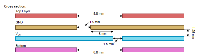
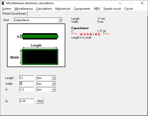
They would like to know if you recommend implementing this interlayer cap, or to just add SMD caps on the top and bottom layers? Any guidance would be appreciated.

Regards,

Antonio

  • Hi Antonio,

    Our ISOW expert will follow-up with you on this within 24 hours, but in the interim we'd like to share some initial thoughts.

    Generally speaking, we'd like to aim for a stitching cap in the region of 30pF to 50pF, or higher. That way, we will get good suppression of higher frequency components ( > ~200MHz). From this perspective, 1.77pF cap as indicated above is quite less and may not be that effective.

    The issue with discrete caps in general , are the ESL ratings. Any (parasitic) series inductance degrades the effectiveness of the cap. This includes both the ESL of the capacitor, and also the inductance of any small traces involved.

    If possible, would it be possible to advise us on the customers targeted Isolation levels, and any PCB board size limitations? This will help us assess if trade-offs can be made to optimize for extra capacitance. 

    Regards,

    Abhi

  • Hi Antonio,

    As Abhi mentioned above, please do let us know what PCB size limitations are. Increasing the area of an inter-layer capacitor is the most effective way to increase its capacitance and preserve the isolation barrier.

    Is this PCB a 1st spin, or has this design previously been tested against emissions standards? If it has been tested before, test data will be helpful to determine whether other emissions reduction techniques can be used in this board instead of the inter-layer capacitor, like common-mode chokes or reducing the power supply.


    Please update us when you have a moment; Koteshwar Rao is following this thread and will provide comments as needed.


    Thank you, and have a great weekend!
    Manuel Chavez

  • Hi Antonio,

    I hope customer is looking into increasing the area of stitching cap to achieve higher capacitance value like Abhi suggested. As also Manuel mentioned, for us to better comment on improvements required in PCB it would be best if you could share us the emissions test results if they are already tested on similar PCB without the stitching cap. Other information like emissions standard pass requirements and end application will also be useful.

    If the requested information cannot be shared here, then you could also send us an email. Let us know, thanks.

    Regards,
    Koteshwar Rao

  • Hi,

    This discussion has moved to internal emails, once we have a conclusion I will come back and post a summary. Thanks,

    Regards,
    Koteshwar Rao

  • Hi,

    The necessary suggestions to improve radiated emissions have been provided over email. The suggestions proposed are similar to the ones in the below E2E post. Thanks.

    Regards,
    Koteshwar Rao