This thread has been locked.

If you have a related question, please click the "Ask a related question" button in the top right corner. The newly created question will be automatically linked to this question.

Vref_A lowest level I/O for LSF0102

Other Parts Discussed in Thread: LSF0102

Hi all,

Page 13 of the datasheet of the LSF0102, it is mentioned that:
<<Vref_A have to be the lowest voltage level across all of inputs and outputs>>

1 - Is this a general statement for the good functioning of the part, or is it only related to the typical application example give in this section of the datasheet?

2 - In case Vref_A is higher than Vref_B, what would happen to the device?

Thanks and best regards,

-nico

  • Hi Nico,

    1. This is good general advice for the functionality of the part. Vref_A and Vref_B have different internal connections (Vref_B is connected to the common gate of the FETs and is considered the device VCC. It should be connected with a 200k resistor in series).

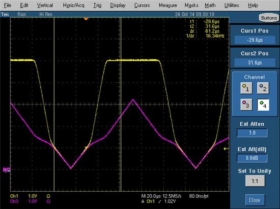
    The LSF acts as a switch when the input is low. When the A-side input signal reaches Vref_A - 0.5 V, the FET starts turning off and is completely shut off by the time the signal reaches Vref_A. Then, the B-side pullup resistor determines the voltage level on the B-side. This is how you get the translation effect.


    Here's a scope shot showing output (yellow) behavior across input (purple) when Vref_A = 1.5 V , Vref_B = 5 V, and the B-side pullup resistor is connected to 5 V. Obviously in practice we'd put a square wave through the part, but the triangle wave shows a voltage sweep. 


    2. If Vref_A is higher than Vref_B, the part will probably not be damaged, but we have seen signal integrity issues. We are actually still investigating cases like these now and will publish an app note on the LSF in the next few weeks.