This thread has been locked.

If you have a related question, please click the "Ask a related question" button in the top right corner. The newly created question will be automatically linked to this question.

Inquiry regarding suitable D-Type Flip-Flop solution for clock dividing

Other Parts Discussed in Thread: SN74LVC1G79, SN74LV163A

Hello, all

Now we have one inquiry regarding suitable D-Type Flip-Flop solution for clock dividing from our customer.

Please refer to the item below, and feedback us with your comment.

We are trying to design clock dividing circuit from 2.4576MHz to 307.2kHz (3.3V).

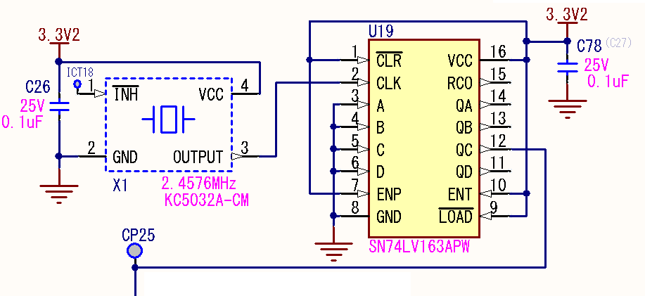
On this case, we assume that D-Type Flip-Flop could simply be used as following device configuration.


Based on this, please let us know which D-Type Flip-Flop solution would be most suitable. 

We thank you in advance for your information. 

Best regards, 

  • If you want to do this in a single part, you should consider using a synchronous binary counter instead of the ripple-carry counter you drew. The part you want will depend on the logic levels and power supply voltage, but something like a SN74LV163A would work. You could also use individual flip-flops in small packages like the SN74LVC1G79. Again the exact part will depend on your logic standard (TTL, LVCMOS, etc.).
  • Hello, thank you for your prompt reply. 

    The logic standard is "CMOS". 

    Then our conclusion is to use SN74LV163A. 

    With regard to this device, we have some additional inquiries from them. 

    Please refer to the items below, and feedback us with your comment. 

    Q1. Please let us clarify about the reason why there are 2 enable pins (ENP and ENT). We would appreciate if you could show the application example for the usage of these pins.

    Q2. Please let us know about the use case of /LOAD pin, since only input A seems to be inverted to the output QA when pulling this pin into low

    Q3. Please let us know about the use case of RCO output. 

    Q4. When using this device for our application, please let us clarify whether all inputs (A to D) and outputs QA to QB could be opened, and then 307.2kHz clock (1/8 divided) could be output on QC and QD. 

    We thank you once again for your information. 

    Best regards, 
  • 1) ENP and ENT are parallel and trickle enables.  This allows you to chain many of these counters and run at or near their maximum clock rate.  For your case I would just tie both of these pins high, either directly to Vcc (this works for CMOS parts, not for bipolar parts like 74LS163A) or through a pullup resistor.  If you wanted to make a large counter using multiples of these devices, normally the first counter would use ENT as the count enable input and its ENP would be tied high.  The RCO from this first counter would then connect to the ENP of all the other counters.  The second counter's RCO would connect to the ENT of the third counter, whose RCO connects to the ENT of the fourth counter and so on.  This means that the "trickle" enables, which go through a lot of gate levels in a large counter, would have 16 clock cycles to settle rather than just 1.

    2) A low level on the /LOAD pin causes the value of A, B, C, D to be transferred to QA, QB, QC, QD on the rising edge of CLK.  There is no inversion.  For your application (clock division) you can just tie /LOAD high.

    3) RCO is the AND of QA, QB, QC, QD, and ENT (note that ENP is not in this equation).  It is used for carry-out when you have more than one of these devices in a chain.

    4) All you really need is a free-running counter.  So you should tie /CLR, /LOAD, ENT, and ENP high.  It's not a good idea to leave inputs floating so unused inputs A, B, C, and D should also be tied either high or low.  For the CMOS chips these connections can be made directly to Vcc or ground.  Unused outputs can be left open.  With 2.4576 MHz provided to the CLK pin, QA will output 1.2288 MHz, QB will output 614.4 KHz, QC will output 307.2 KHz and QD will output 153.6 KHz.  It is not possible to output 307.2 KHz on more than one pin with this device.

  • Hello, thank you for your continuous support. 

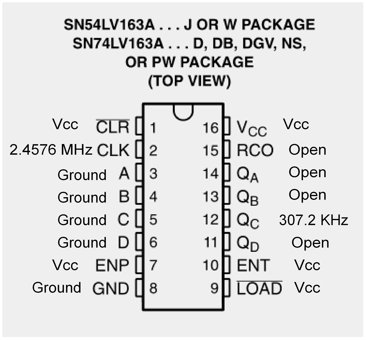
    As a conclusion, they have decided for the usage on this device as below;


    Best regards, 

  • That looks correct.  Unused outputs including RCO can remain open.  The only thing I would add is to keep the 2.4576 MHz net very short.  By short I mean 1 inch (25mm) or less.  If for some reason the oscillator cannot be placed next to the SN74LV163A, then I'd add a series resistor on the output pin of the oscillator to allow you to match the trace impedance and reduce ringing if necessary.  Also I don't see a specification for rise and fall time for the SN74LV163A, but it would also be a good idea to keep the output net from QC as short and direct as possible, and add a series resistor if this net needs to be more than about 4 inches (100mm).