This thread has been locked.

If you have a related question, please click the "Ask a related question" button in the top right corner. The newly created question will be automatically linked to this question.

SN74LVC1G17: SN74LVC1G17

Part Number: SN74LVC1G17

Hi,

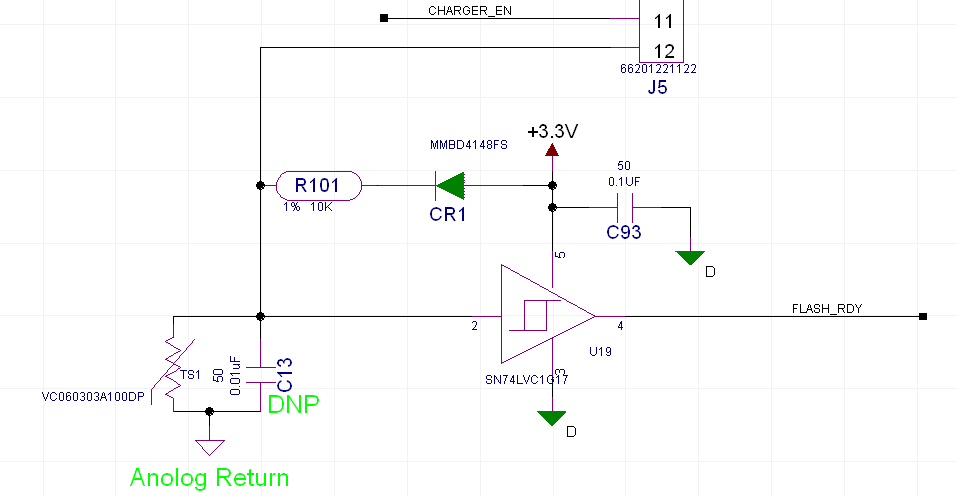
We are using SN74LVC1G17 to protect one signal that is crossing the board. We know that the signal has some spikes due to noise on the the source signal.  The source output is an open drain signal on a flash board. The schematics is as following. 

The Analog GND and DGND has a single point connection on the board. The TS1 starts clamping around 5V, and clamps at 12V.

Recently, the input (pin2) of U19 constantly get burned.When it is burned, the resistance is about 30ohm from pin2 to pin3. We checked input. The source signal comes from the flash board has a spike at about +/-120V for about 5us to 10us when the flash is triggered. The frequency is about 3Mhz to 5Mhz. The noise is coupled into the input, but there's not much energy at all. The chip is designed for ESD protect, and should be able to handle the spike. I'm scratching my head, what could possible cause the failure?

Any suggestion is appreciated.

thanks

Peng

  • Here is what the designer's guide of a similar family (AHC) has to say about voltage spikes:

    Input voltages greater than 7 V must be avoided to preclude damage to the gate oxide of the input stage. This damage is not necessarily permanent, but will adversely affect the expected lifetime of the circuit. The gate oxide of AHC devices is only 200 Å thick. An input voltage of 7 V corresponds to a field strength over the gate oxide of 350 kV/cm. Although breakdown of the oxide is expected only at input voltages above 10 V, electrons tunnel increasingly into the gate oxide at field strengths greater than 350 kV/cm, influencing characteristics of the transistors and causing failure.

    The chip's ESD protection is designed for discharges that could happen during manufacturing.
    A typcial ESD discharge is a single event, but your megahertz pulses that last for several microseconds sound like a lot of energy.

    What is the purpose of CR1/R101? If it is for protection, there should be no resistor.

    Anyway, it appears that TS1 is not fast enough, or does not clamp low enough. I'd recommend to add a series resistor of about 500 to 1000 Ω between TS1 and U19.

  • CR1/R101 is for protection. R101 was there because the source is an OC. Without R101, there will be lot's of current on CR1 during the input low.


    How long is the duration of an ESD pulse?.

    thanks
    Peng
  • R101 prevents the protection from being effective, and the diode is in the wrong direction. To protect against negative voltages, use a diode from GND to the signal. To protect against positive voltages, use a diode from the signal to VCC. To ensure that these diodes switch before the chip's internal diodes, use Schottky ones.

    The standardized ESD test pulses are specified by their charge; how fast they dissipate depends on your circuit. However, see MSP430™ System-Level ESD Considerations (SLAA530) for examples.