This thread has been locked.

If you have a related question, please click the "Ask a related question" button in the top right corner. The newly created question will be automatically linked to this question.

SN74AUP3G14: Input transition rise or fall rate

Part Number: SN74AUP3G14
Other Parts Discussed in Thread: SN74AUP1G14

Hi,

I have used SN74AUP3G14 in one of my logic circuits and is powered with 3.3V. However, I have a RC  timing network in its input due to which the input transition time is extremely slow. The input will rise and fall from 0V to 3.3V in about 25 seconds. I used it in this way as the SN74AUP3G14 has schmitt inputs. I looked at its datasheet, but in the revision history section, it said that "Deleted input transition rise or fall rate (Δt/Δv) paramater from Recommended Operation Conditons table". So, my question is will I be able to use it with such slow rise and fall rates? Will it impact any damage to the SN74AUP3G14? Or will there be any abnormal performance of the logic gate? Please help.

Thanks.

  • Hi Bhargav,
    A slow input will not damage the SN74AUP3G14, however it will use much more current than what is specified in the datasheet. Note that the Icc specification is rated with inputs at GND or Vcc, and ΔIcc is rated at Vcc - 0.6V. Maximum supply current will be around V_I = Vcc/2.

    The Δt/Δv was likely an error when updating the datasheet from the original format to our new format, and was removed because Schmitt-trigger devices do not need that spec.
  • Thanks a lot for the quick response. So my understanding is that, ΔIcc = 50 uA as given in specs. So, as long as the input is below Vcc-0.6 V, the current consumption is about 50 uA and as soon as the input will be equal to Vcc or completely 0 V (GND), the current consumption will fall back to 0.9 uA. Am I correct?

    Thanks again.
  • Yes; those are the worst-case upper limits for the specified test conditions. In between, the current is worse.

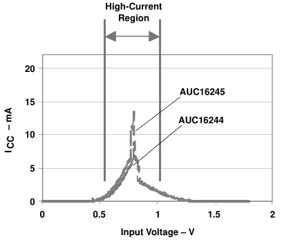
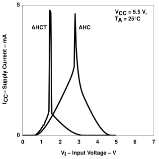
    The actual current consumption depends on how much the upper and lower input transistors are opened. Within about 0.6 V of GND or VCC, the input voltage does not yet reach the gate threshold voltage of either transistor, so the current is essentially zero (you get only leakage current). The farther away you get from the rails, the larger the current becomes; it has a maximum at about the middle.

    There is no such graph for the AUP family, but all CMOS inputs behave essentially the same; this is for AUC at VCC = 1.8 V and AHC at VCC = 5.5 V:

    (The sharp spike is an artifact of the Schmitt-trigger action.)

  • Hi Bhargav,

    To be clear, 50 uA is _not_ the maximum Icc for this device.  That is only at Vcc-0.6V.  I took a plot of the single channel version of this device (SN74AUP1G14) to show how the current behaves across different voltage inputs.

    Each color represents a different supply voltage.