This thread has been locked.

If you have a related question, please click the "Ask a related question" button in the top right corner. The newly created question will be automatically linked to this question.

SN74HC240: Low-level input voltage not according to datasheet

Part Number: SN74HC240

We use  SN74HC240DWR chip and I recently tested the input behavior and found the Low-level input voltage to be 1.320V at 5V supply voltage.

The measurement was taken at a 1K Ohms SMT resistor at frequency of 2 Hz with 80% duty.

(So the measurement was not directly on the chip input - but on the separating 1K resistor, where my function generator 50 Ohm output was connected. Voltage measurement was verified to be accurate.)

The datasheet shows the Low-level input voltage to be MAX at 1.35V at 4.5 Vcc. Subsequently I measured Low-level input voltage on another device to be higher, at a lower Vcc!

This surprised me. At the same measuring setup, with 1K resistor and Vcc = 3.3V - the Low-level input voltage was 1.420V. Why is this happening?

The datasheet is SCLS128D − DECEMBER 1982 − REVISED AUGUST 2003 shows progression on the Low-level input voltage in function of the Vcc (see table page 3)

So why aren't the devices behaving like that? Did anything change about those chips since the datasheet was made in 2003?

If so - what are the input differences? Specifically - what are the values of the Low-level input voltage for Vcc of 3.3V and 5V for those newly produced devices?

  • Hi Andrew,

    Can you give us a schematic of your test setup please?

  • I soldered a 1K resistor to an input of the SN74HC240DWR on pin 15 (2A3). Then, to that 1K resistor - I soldered a test point, where I attached a scope probe and generator output. The chip has either 5V or 3.3V connected with a ceramic cap on the power pin 20 and grounded on pin 10. I pulled the remaining inputs to Vcc. OE is low. That's it.

    The test is basically to feed the 2Hz waveform in state when the buffer output is Low. At that point the input state is always High. The waveform length is 0.5 seconds - and the 20% of that is negative going impulse. That impulse lower voltage is my triggering pulse. I change the waveform offset - to move that impulse lower gradually. I measure the lower edge of the impulse using scope. At some point the buffer changes the state to Y output H on pin 2Y3. That is the voltage I reported as Low-level input voltage. It is not what the datasheet says it should be. 

    Regardless of my test - what is the stated Low-level input voltage for 5V and 3.3V - even without going into my testing?

    Is there a newer reliable datasheet?

    Thank you

    Andrew

  • I will definitely look into this and post my results. It will take a few days for me to get samples.

    Just out of curiosity, is there a reason you are testing the VIH/VIL specs of this device? Are you planning to use it in a particular application?
  • We are already using the part. I think the current use is 40k pieces annually. This test was made because we discovered some external issues, so the concern is mainly about the listed parameters in the old datasheet not the part itself. I am worried that there may be some variation - and one day the devices will have a lower threshold for the VL and the part will stop working. That would be a big problem.

    It is very concerning to me - that the threshold voltage did not follow the datasheet - because since the 4.5V maximum value is listed at 1.35V therefore I expected to see VL=1.5V at 5V Vcc not the 1.320V that I measured. I mean that is strange but not very much off and I could understand that as a part variation. I could argue - it would be OK - but then imagine my surprise when the Vcc was lowered - and I expected to see maximum of VL=1V but the measured value was higher at 1.420V - so the VL went up on me on the second device - which I did not expect at all.

    I can't explain it otherwise than there is an error somewhere. I calibrated my measuring setup with an external meter and DC source - and the measurement is solid. The waveform is practically a DC type of behavior at 2Hz. The test impulse length is basically 100 ms. Error is not here. There must have been a change to the IC architecture - because the devices don't seem to follow the Vcc changes. It is either that - or the devices have some variation that I cannot explain. I really can't speculate on the causes of such behavior and that is why I am asking.

    I will rely on your provided data. The VL you measure at 5V and 3.3V and maybe subsequently at values provided by the datasheet: 2V, 4.5V and 6V to be able to compare that to the datasheet.

    I need an official measurement and explanation of this issue if we are to continue using this part.

  • Thanks for the detailed explanation Andrew. I have the parts on order and will test them as soon as they get to me.
  • Hey Andrew,

    I was able to get into the lab today and test this on 6 devices.  I used linear interpolation to find the appropriate VIH and VIL values to test at 3V, 3.3V, and 3.6V:

    VIH

    @3 V = 2.16 V

    @3.3 V = 2.358 V

    @3.6 V = 2.556 V

    VIL

    @3 V = 0.84 V

    @3.3 V = 0.942 V

    @3.6 V = 1.044 V

    I found that all devices I tested worked at better than the datasheet specs. Here's a couple scope shots from my testing:

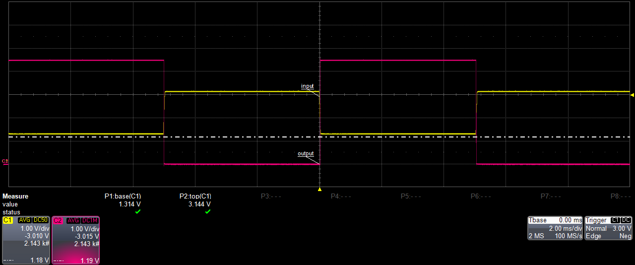
    At 4.5 V operation:

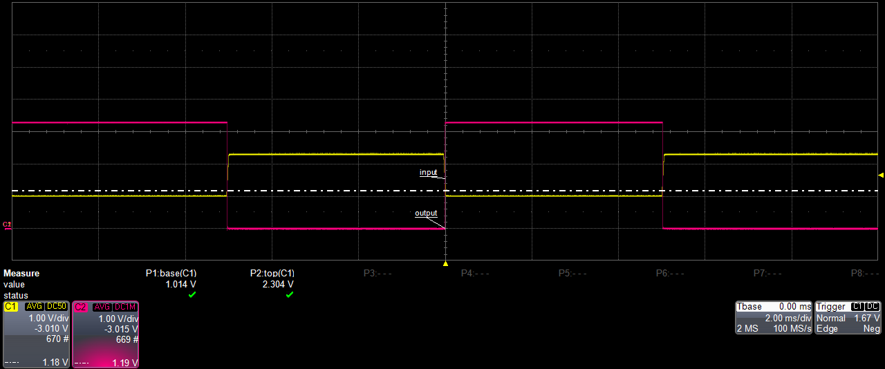
    At 3.3 V operation:

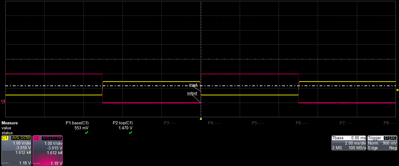
    At 2 V operation:

    It seems that what you have measured is not common to all of these devices.  I would recommend opening a failure analysis with your local TI sales office to get to the bottom of the issue.

  • Thank you Emrys for your analysis - I would like to ask about the second graph "@3.3V operation" - the yellow line indicating the input is set to 1V/DIV and looks like the lower part of the pulse is at exactly 1V level. Am I correct?

    So how did you get the value of  VIL @3.3 V = 0.942 V - if the chip clearly changed state at 1V? (If the 0.942V is an interpolated value - then it is not confirmed by the graph.)

    If the VILis indeed at 0.942V then the yellow line is not reaching that - so how did the chip changed the logic state?

    (It looks like your chip responded at a higher level - but it is hard to say where exactly - without zooming into that area there) 

    Could you be so kind and show the logic shift area at 100ns/div to show when the chip starts to respond to that falling edge of the signal?

    I will redo my measurements again - and I will use your setting of pulse length of 5 ms because clearly this is different than what I saw.

    I am not seeing such a low VIL levels as you provided. I don't see 0.942V - that's not happening on my end.

    My signal started to change the logic at much higher voltages.

    My measurement was at 1.420V  - which is basically a little below the value of your triggering point located at 1.67V - little above that dotted line at 1.18V and below the level of that yellow arrow on the right.

    Thank you

  • I placed a measurement of the low and high value for the input on the scope (shown as "P1: base(C1)" and "P2: top(C1)".

    I think there's some confusion on terms here. VIL is not a lower threshold value; it is not the voltage at which the device will switch. It is the largest value at which TI guarantees this part will recognize the input as a logic LOW. Note that I calculated a VIL value of 0.942V, however I tested at a higher value of 1.014 V -- indicating that the device can definitely be used at or below the datasheet spec of 0.942 V (linearly extrapolated from the given 2V and 4.5V values).

    This device is not designed to operate near the thresholds - thus why it has VIH and VIL values in the datasheet instead of VT+ and VT- values (which would be positive-going threshold and negative-going threshold, respectively). There is also a recommended operating condition spec for the transition rate from a 'LOW input to a 'HIGH' input, which is called "∆t/∆v Input transition rise/fall time Input transition rise/fall time" and in the worst case, indicates that the device should be switching between VIL and VIH in under 1000 ns.

    TI currently does not, and has no plans in the future to, spec the threshold voltage of standard CMOS devices. We do, however, spec the threshold values of Schmitt-trigger devices.
  • This is very helpful, than you. You said the devices behaved a little better than the 0.942V. I understand. Thank you for giving me the 1.014V measurement. That was the number I was looking for. I will now remeasure samples on my end to make sure my numbers match. I will get back with you with my results and we will take it from there. Technically - my voltages were higher, therefore they matched the minimum threshold.