This thread has been locked.

If you have a related question, please click the "Ask a related question" button in the top right corner. The newly created question will be automatically linked to this question.

SN74LVC1T45: Request for schematic/layout review

Part Number: SN74LVC1T45
Other Parts Discussed in Thread: BQ25895,

Could you let me know how I can contact for schematic/layout review?

One side is 2.8V, and the other side is a battery voltage and an active-low switch (nominal y 3.9V)

I'm trying to make certain the level is properly translated as well as there is no leakage from the battery to the 2.8V side when the 2.8V LDO is off.

Thanks,

Andrew

  • Hi Andrew,
    Please post your schematic and we will be happy to take a look.
  • Hi Emrys,
    Would it be possible to email you the schematic? Or send you a PM?
    Regards
    Andrew
  • Hi Emrys,

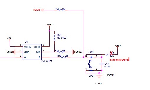
    I've summarized my questions in the attached Powerpoint.

    Basically I'm trying to "isolate" a button, which is pulled up in off state, from the MCU.

    When "On", the MCU will have an interrupt running to see how the button is pressed: short click, long pause, ...

    When "Off", the only purpose would be to turn on the charger IC, BQ25895, by going active low on the button.

    Thanks for your review.

    Regards,

    Andrew

    questions ti lvl shfter.pptx

  • Hello Andrew,

    In your description, I see that you have a non-TI part, don't know if that is just a matter of what you might have available in your library, but I can tell you that the TI part number is SN74LVC1T45. 

    For our device, we have a VCC isolation feature, which means that if either VCC is grounded, then all outputs are in the high-impedance state.

    From what I can tell, this is what you are trying to do, so yes, if you put VCCB to GND, then the outputs will be tri-stated.

    If both VCC lines are present, then the MCU will be able to read the B line without any issues.

    Best,
    Michael

  • Michael,
    I appreciate your feedback.
    My apologies for the part number. I just assumed that the part was from TI.
    We will take a look at SN74LVC1T45.
    Regards,
    Andrew
  • Hi Michael,
    After discussing with the TI's charger IC team, here is what I have found.
    QON can be several values depending on operating mode.
    1. Vqon = BAT for battery only mode
    2. Vqon = 5.8V when Vbus is 9V
    3. Vqon = 4.3V when Vbus is 5V

    Rqon = 200k ohm

    If we ties VCCB to VSYS, the voltage range would be 3.5V to 4.5V. But the B pin voltage could be as high as 5.8V. Having said this, we may limit the use cases to 5V USB. Still we may be in a situation Vb may be higher than VCCB. Overall the operation is a human action so the speed is not an issue.

    Another option is, the VCCB may be off in the Off state. and tie it to 5.5V off the buck/boost regulator, which turns on after the unit powers on.

    Thanks,
    Andrew
  • Hi Michael,

    I did some measurements on our previous board.

    I removed the resistor to VBAT so the SW1 is connected directly to nQON of BQ25895.

    Here’s what I measured.


    Power Input

    Battery voltage

    PMID

    Vsys

    SW1 (high side)

    “9V” USB adapter


    8.74V

    4.2V

    4.58V

    “5” USB adapter


    5V

    4.2V

    3.2V

    Batter only

    4V

    5.12V

    4.0V

    2.8V


    The PMID voltages make sense.  Vsys seems to be cap’d at 4.2V with USB input and in battery only mode, it follows the battery voltage

    The nQON voltage seems lower than what I expected.

    Regards,

    Andrew

  • Hi Michael,

    My apologies.
    Here are my thoughts.
    Our new design ties VCCA to 2.8V. I am thinking using 2.8V for VCCB as well.
    Then the voltage at B pin will range from 2.8V to 4.6V which is below the operating range.
    The only caveat would be the Vb would be higher than VCCB.

    The other option is to tie VCCB to Vsys.
    However, I am concerned that in the battery only mode, SW1 can only be at 2.8V, which is 0.7 x VCCB.
    According to the datasheet, 0.7 x VCCB may be the min Vih.
    Did I understand correctly?
    Regards,
    Andrew
  • Hello Andrew,

    Got your message, and posting here:
    ""I think I can summarize my question now as I understand the part better.

    Direction: B to A
    VCCB: 2.8V
    Voltage range on B: 2.8V to 5V
    So the question is the voltage level on the B pin can go above VCCB as long as it stays below 5.5V.

    I am thinking this is ok from signalling perspective as the B side is input.

    I appreciate your help.""

    In summary, yes, if the B side of the device is set to be the input, which it is in your system, the input voltage into this pin can be any voltage up to 5.5V even when your VCCB is at 2.8V.
    So you can power VCCB any range between 1.65V and 5.5V, and that input could tolerate any voltage up to 5.5V.

    This device is what we call over-voltage tolerant at the inputs.
    Hopefully that helps to address your concerns/questions, please let me know if you have additional questions and I would be happy to help!

    Best,
    Michael