This thread has been locked.

If you have a related question, please click the "Ask a related question" button in the top right corner. The newly created question will be automatically linked to this question.

CD4047B: Pin 10 maximum output current/power

Part Number: CD4047B

Hi, team,

I have one question about CD4047B pin 10 output power.

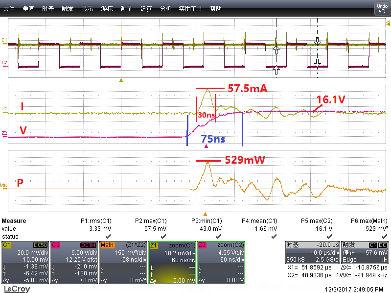
Customer tested the pin 10 voltage and current, shown in below waveform. The peak V*I is 529mW, time period is 30ns.

Is there any risk for CD4047B pin 10 and device?

What is maximum current and power requirement for CD4047B in this short 30ns time period?

Thanks.

Johnny

  • Hi Johnny,
    It would appear that the trace "Z2" is the output voltage of the device. If that is the case, the power measured would be the load power, not the transistor dissipation in our device. The correct voltage to measure would be from pin 14 to pin 10 ( V(VDD) - V(Q) ).

    The maximum internal transistor dissipation is 100mW. Based on the above, and assuming that the output voltage is being measured (not the transistor voltage), there shouldn't be any problem.