This thread has been locked.

If you have a related question, please click the "Ask a related question" button in the top right corner. The newly created question will be automatically linked to this question.

SN74GTL1655: Output abnormal signal

Part Number: SN74GTL1655

Hi team,

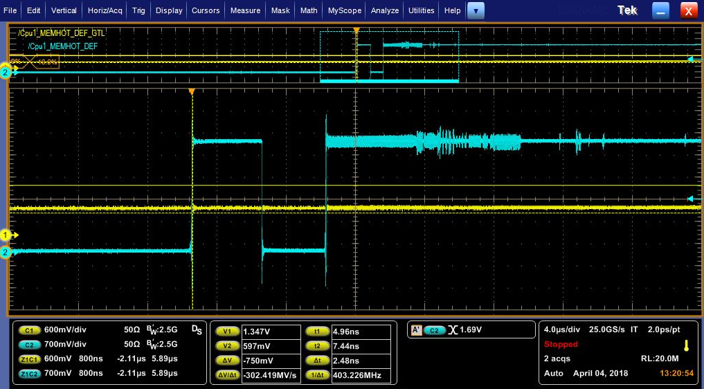
My customer find that after powering on the chip, the output of A port will generate a serial of random signal when the B port is logic high.

The schematic is as below:

And the output signal is the purple one.

Could you help to review the schematic and make your comment to this problem?

Lacey

Thanks a lot!

  • Hi Lacey,
    Can you tell me what the other signals are on the scope shot? What is connected to each end of that channel?

    Since today is a holiday, we probably won't get back to you until Monday.
  • Hi Emrys Maier,
    The port B is connected to CPU I/O pin and the port A is connected to CPLD。
    I am not very sure what the other signal is.
    And I can make sure is that the problem exists only when we input a logic high to the port B and when the voltage increase to 600mV.

    Lacey
    Thanks a lot!
  • Hey Lacey,
    If you can get a clean scope shot showing the input, output, supply, and ground (all measured at the device) it would be very helpful. I'm not really sure what's going on in the above scope shot, so it's hard to comment.
  • Hey Lacey,
    I'm going to close out this post until I hear back from you. All you have to do to re-open is to reply, and that will get my attention.
  • Hi Emrys,

    Below are the signal I got from customer.

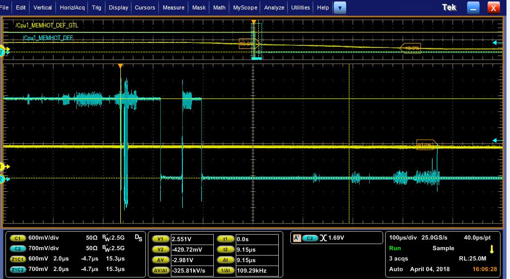
    The yellow one is the input signal, and the blue one is the output signal.

    When the input signal turn from 0 to 1, the output signal will show out a random signal and also a high overshoot.

    When the input signal turn from 1 to 0, the output signal also show out a random signal and a high overshoot.

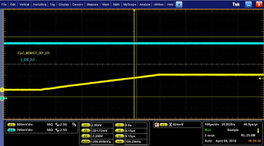
    Also, customer has measure the input signal and the 3.3V power supply.

    Yellow one is the input signal, blue one is the power supply.

    The random signal of the output happened every time when the input signal has a change(such as from 1 to 0 or from 0 to 1).

    So can you help to comment about the cause of the random signal of the output and the method to solve the high overshoot in output signal?

    Lacey

    Thanks a lot!

  • Hey Lacey,
    I've asked our local translation expert to look into this. He's out for today, but you should expect a response tomorrow.
  • Hi Lacey,

    Which input signal is the scopeshot in the yellow?
    I am suspecting the slow input transition on the input is causing the output to behave this way.
    Do you have the current consumption value from the supply as well?

    For the overshoot, I suggest to have a small series resistor on the trace to dampen it. It is most likely caused by driving the output into hi-z input.
  • Hi ShreyasRao,
    The input signal is the yellow one in the below picture. The transition time is about 400uS.

    And the blue one is the supply voltage. Customer said he didn't have the consumption value. But from the picture, it shows the 3.3V voltage is stable when the abnormal output signal happened.

    Does the consumption matter?

    Do you have do the same test in your lab? If so, can you send me the test results, I can compare with the condition of customer.

    Another question:

    For the question of the overshoot, can you help to indicate the change and the resister value in the schematic?

    Lacey

    Thanks a lot!

  • Hi Lacey,

    Is there a possibility of increasing the transition time? I am concerned that the transition time in 100s of uS can affect the output signal.
    The current consumption would indicate that the device may be stressed during the transition of the input.
  • Lacey,

    Having a 100ohm series resistor may be a good start. It should provide the impedance matching while limiting the overshoot.
  • Hi Shreyas,


    I have confirmed with customer that they cannot change the transition time because it depend on the reference supply voltage.

    Can you help to do confirm the problem is caused by the low transition time?

    In addition, customer feedback they wants to try to reduce the drive capability to reduce the effect of the output random signal.

    But the situation is that they can not change the PCB layout, so can you give your recommendation to reduce the output drive capability according the customer's schematic I have attach before.


    Lacey
    Thanks!

  • Hi Lacey,

    www.ti.com.cn/.../slla364a.pdf

    The app note discusses the slow input transition rate issues causing oscillations on the output.
    I would suggest to try 20ns low to high transition time on the input signal , if possible , to see if the output stabilizes as an experiment.
  • Without changing the PCB layout it is hard to recommend anything to reduce the overshoot / undershoot.
    I do not know what is the GTL driving to, but i would see if the receiver is overvoltage tolerant to accept the overshoot above its operating Vcc. It may not be an issue as usually the receiver devices will have sufficient tolerances built in to accept the variation on the its input for such short duration (in ns).
  • Hi Shreyas,
    Thanks for your reply!
    I will feedback your comment to customer.
    What can I help for solving this issue?

    Lacey
    Thanks a lot!
  • Hi Shreyas,
    Since customer can't do the test to comfirm this problem is caused by the low transition time. Can you help to reproduce the problem in the lab and send me the results by email. Customer need this to clarify the issue.


    Lacey
    Thanks a lot!
  • Hi Lacey,

    I will have to order the parts and then find the appropriate socket to test them. I am not sure if we have the right socket for this device or not currently.

    I will update you more once I get the devices and the sockets. 

    I will plan on showing the behavior of the device under normal conditions and inputs. The response should ideally be better than the oscillations and random signals the customer is currently experiencing.

    Meanwhile, if there is any other update from the customer, please let me know as well.

  • Hi Shreyas,

    1. Can I find the transition time spec in the datasheet?
    2. In addition, customer asked if we have the GTL part integrated with the Schmitt trigger?

    I have searched the TI.com, but I cannot find one.

    or do you have the roadmap for the Schmitt trigger input?

    Lacey

    Thanks a lot!

  • Lacey,

    Thank you for looking into the parametric search for the device. I do not see GTL devices with Schmitt trigger internally built in.
    It might have to be externally included.
    The transition time for the power supply ramp rate is specified but there is no specification for the input transition time.