This thread has been locked.

If you have a related question, please click the "Ask a related question" button in the top right corner. The newly created question will be automatically linked to this question.

CD74HC4046A: CD74HC4046 phase discrimination output problem

Part Number: CD74HC4046A

Hi all,

One customer use CD74HC4046 to make phase discrimination for two signals (1 hz). He wants to take advantage of  the signal PC2out  after filter as VCXO control signal. When PC2out disconnect to any devices, the phase discrimination signal can be seen obviously. But when a RC low-pass filter connected after PC2out, the phase discrimination signal will disappear, the filter output is close to zero.

In normal condition, the DC voltage after the filter should be close to 1V, but it is not clear why he lost the phase discrimination output signal after connecting with RC filter. The RC filter parameter is R=10k, C=10uF, because the input is 1Hz signal, so the RC bandwidth is very low.

Could you explain the root reason that may cause this issue and tell the method to solve it? 

Thank you.

  • Hi Lenna,

    It's likely that a 10kohm resistor and 10uF capacitor aren't large enough to properly filter the output, and the timeframe for change is also likely very large.  I think a simulation can easily illustrate the problem.

    I have created a 10% duty cycle waveform operating at 1 Hz, then I filtered it two different ways (10kohm, 10uF and 100kohm, 47uF)


    VG1 is the source, or "Vin"


    Note that since the duty cycle is small (ie the phase difference is small) the output drops to zero after every output pulse. It will never create a DC average due to the limitations of the filter.

    With larger RC values, the output can be filtered, but it takes about 20 seconds to level off.

  • Hi,

    Actually, the R and C already have been set to 100k and 10uF.
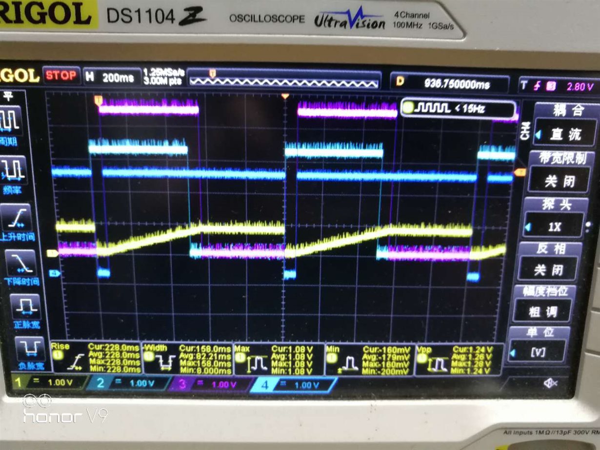
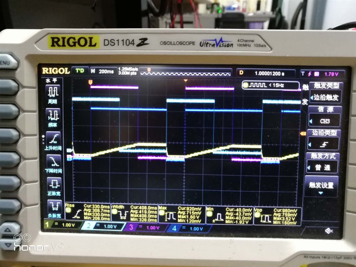
    According to the test results, the main problem is that the rise time of PC2out is different from that of the fall time. The RC parameter is the same, and the rise time of PC2out is much longer than the fall time.
    The causes that PC2out's level is quickly pulled down to zero as long as PCPout is low.
    Here are two sets of test waveforms:
  • Hi Lenna,
    Is this the same issue being described in this thread:
    e2e.ti.com/.../687707

    ?
  • This is a question post on E2E China. The pictures look the same. Maybe it's the same person's issue.
  • Hi Lenna,

    I believe the issue could be related to the incoming signals. The PC2 phase comparator uses rising edges of each signal to compare phase, however this  method of phase comparison can be problematic because the device can become 'confused' and invert the desired output.

    In normal operation, the SIG_IN and COMP_IN (VCO_OUT) signals will have their phase compared and output a short 'high' pulse for a phase lead condition, and a short 'low' pulse for a phase lag condition.

    It's possible to get into a condition where PC2 confuses which signal is leading or lagging because it is only looking at the rising edges.

    This can become reversed if one signal is applied before the other and the phase is not what is expected.  The above signal timing diagram shows how the output could be held low regardless of the output.

  • Is this happening on all units, or only some? When replaced with a new unit, does the problem persist?
  • I'm sure that the incoming signal Sig_IN  is right, in fact, the sig_in is GPS_PPS, and the Comp_IN is the divieded 1Hz signal from VCTCXO, so they are both 50% duty cycle signal. The PC2Out signal seems to be right when pulse out, now the only problem is the falling time of the pulse signal. The falling time is obviously shorter than the rising time, so the filtered signal can't accumulated to the expect level to control the VCTCXO.

  • yes, it is happening on all unit. I have changed the unit, but the problem persist
  • Hello Mingtao,

    I have looked closely at the waveforms, and I still believe that the device is becoming "confused" from the inputs.

    Note that in the waveforms above, PCPOUT is HIGH for the majority of the time, and only LOW when the output is driving LOW.  This indicates that the output drivers for the CD74HC4046 are turned _off_ (ie in high impedance mode) during the time when the signal is slowly rising or holding steady.

    This is the result of the COMPIN being triggered first, which forces the output low. When SIGIN triggers, the output is put into high impedance, then the next cycle this happens over again -- the device never charges the capacitor because it is attempting to correct the phase misalignment by driving the VCO control input LOW. The output appears to have a small leakage current that is charging the capacitor up to a specific voltage (not sure if this is coming from the opamp or the HC4046).

    Since you are using a 50% duty cycle signal on both channels, can you use PC1?  This would eliminate the need for sequencing the inputs correctly by using and XOR comparator rather than the edge controlled comparator.

  • "This is the result of the COMPIN being triggered first, which forces the output low. "    I agree your point and the PC2out logic function is right(JK flip-flop) .

    But the question is the falling time is obviously short. According the RC time constant, the falling time of the pc2out should be the same as rising time. During the 1PPS cycle, PC2out voltage level rise up for about 50% duty , then stay for about 30% duty, and then fall down for about 20% duty. In theory,the Pc2out level will be a certain level but not 0 level 

    the problem of using PC1  is that the phase difference is 90 degree not 0 degree when the pll has locked  

  • Is there anybody can give me some other suggenstions about the problem?  

  • Hi Mingtao,

    Perhaps I can explain another way.

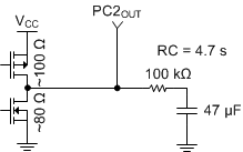
    The output impedance of the CD74HC4046 when outputting high is ~100 ohms, and when driving low it is ~80 ohms.  Let's draw the output with your filter values:

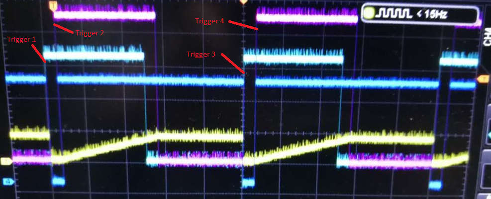
    Now, let's closely look at your PC2_OUT waveform from the above posts:

    I have labelled four rising edges so we can discuss the signals.

    Per my previously explained post, at Trigger 1, the output is driving LOW, which means the CD74HC4046 is connecting the PC3_OUT pin to ground with an impedance of about 80 ohms. This is normal operation of the device.

    At Trigger 2, the output goes into a high impedance state (> 1 Mohm).  Note that the output is not forced immediately high, but it very slowly rises (over about 0.5s).  I believe this to be caused by leakage current through the device, probably related to the purple signal shown.

    When the purple signal drops to zero, the output holds at the previously charged level, as expected for a high impedance output.

    If the output were driving HIGH, then the output pin would immediately drive to Vcc, which is not what is happening.  As I have previously stated, the device is 'confused' and thinks the wrong signal is leading.  The best way to fix this is to force one signal to start before the other.

  • sorry, I have made a mistake about the signal meaning. The yellow one is the filtered signal about PC2out but not PC2out itself.
    so the rising part coresponds to the charing of the 10uf capacitance through the 100k resistor, then the falling part shoud coresponds to the discharging of the capacitance. In theory, the falling part should as slowly as rising part, and then the voltage drops to a certain level but not zero.
  • Unless you have a connection or component that you also didn't tell me about, what you're saying is not possible.

    The CD74HC4046 cannot reduce the resistance of your 100kohm resistor.... even if our device somehow magically had 0 ohms of resistance to ground, your cap will still have to discharge through the 100kohm resistor. You may want to check your measurements and connections again.