This thread has been locked.

If you have a related question, please click the "Ask a related question" button in the top right corner. The newly created question will be automatically linked to this question.

CD74HC4059: Creating a Frequency Divider

Part Number: CD74HC4059
Other Parts Discussed in Thread: SN74LVC1G17

Hello! 

I've developed a frequency divider using the said part number based on the help of a previous thread. Though, we only discussed the J and K pins on that thread, and nothing else.

Notes:

  • I am basing the configuration on the assumption that "high" refers to Vcc, and "low" refers to GND
  • I currently have the device set for mode 2
  • N=15, Vcc = 5V, freq_in = 500 Hz (connected to pin 1, CP) square wave
  • The J and K pins are connected directly to Vcc or GND depending on the pin (no resistors are being used)
  • Latch Enable (LE pin 2) is connected directly to GND
  • This circuit is created on a breadboard and I am using a SOIC to DIP adapter

My Issue:

  • I am not receiving any output signal with LE connected to GND
  • If I connect LE to Vcc, I receive an attenuated version of the input signal (same frequency, less voltage)
  • If I leave LE floating, I do not receive any output signal

Please help! I am not entirely sure what to do with the LE pin. 

Thanks in advance,

Gage

  • Hi Gage,

    Yes, Vcc = HIGH, and GND = LOW.

    From the datasheet:

    A “high” on the Latch Enable input will cause the counter

    output to remain high once an output pulse occurs, and to

    remain in the high state until the latch input returns to “low”.

    If the Latch Enable is “low”, the output pulse will remain high

    for only one cycle of the clock-input signal.

    For your application, I would recommend setting LE = GND.

    Can you provide a schematic for your test setup?

    Also, if you have scope shots for your input signal and the output you are seeing it would be helpful.

    Since your signal is very slow, make sure to get a zoomed in view of the edges (rising and falling) for the input.  We are looking for fast/sharp input edges.

  • Hey Emrys!

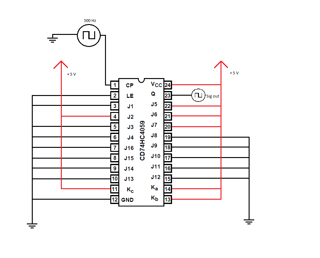
    Please see the attached photos for the schematic, and pictures of the signal. One image shows the input signal at 0.5 ms/div and the other scope image shows one pulse at 0.15 ms/div.

    Thanks,

    Gage

  • I haven't seen a tube scope in a while (since my days in the USAF). Is it possible to get an image of the rising edge at ~100ns per division?
  • Emrys,

    First off, thank you for your service. Secondly, I think that the picture shown below is the best one I will be able to get you. I used a cheap digital scope to acquire this screen shot. It is shown at 2 us/div.


  • Hey Gage,
    Thanks.

    That's what I was afraid of -- the CD74HC4059 uses standard CMOS inputs, and those don't do so well with slow inputs (rise time here looks like ~7us). The maximum total rise time is listed as 500ns (for 4.5V operation). We typically recommend staying below 100ns.

    I'm not certain if that is causing your troubles, but it definitely will cause problems for the HC4059 including internal oscillations, excessive current, and possible internal damage. All kinds of weird stuff can happen.

    The fix should be relatively easy though - just add an HC or LVC schmitt-trigger buffer (ex: SN74LVC1G17) prior to the input should clean up the signal.
  • Great! That sounds easy enough to try. I'll order that part from Digikey ASAP, and I'll try it out.

    Cant thank you enough for the help that you've been.
  • Hi,

    I installed the schmitt-trigger before the circuit, and it seemed to make the output more consistent, but the "divide-by" number seems to be much larger than expected. I set N=15, and with an input frequency of 500 Hz, the output frequency was about 1 pulse per 4 seconds. Thoughts?

  • Sounds like it's dividing by ~2000 instead of 15. Since you have the circuit built, I'd recommend swapping some bits individually to see what happens -- I could do this as well, but I'd have to order samples, build the circuit, and play around with it, which would take at least a week or two based on my current work load.

    I would start with the 'mode' bits and then try the 'ones' place to see if it's making a change as expected. There's always a chance there's a mistake in the datasheet -- I've never built a circuit with this device and just had to go based on what the D/S says.
  • I've done some experimenting the last few days. I looked over the example given in the DS and the realized that we made an error. In Mode 2, J1 is the only input for the remainder, therefore when I had J2 = H, it considered that jam to be in the 1000's place.

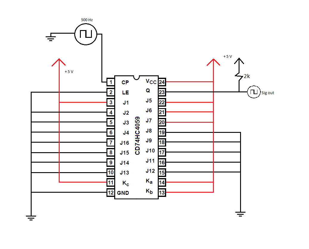
    I just rectified this problem, but now I'm thinking about another issue: the output signal is pretty noisy. I have 36058 RPM at the input, and the output is jumping around 3200 +/- 1000 when it should be 2400 RPM. I played around and installed a 2k resistor between output signal and Vcc, and this seemed to help a bit, but not enough. Now the output signal bounces between 2500-2800 RPM. I've tried different valued resistors, but they either seem to make the noise worse, or make the signal drop to 0 V. I've also tried installing a cap in-place of the resistor, but it didn't help. Maybe I should try a cap and resistor in parallel? 

    Here's the interesting part: if i touch my tube scope to the output, the signal becomes much more stable and hovers around 2500 +/- 10 RPM. Thoughts?

    Take a look at my new circuit below:

  • Hey Gage,
    I've been on vacation for a few days - sorry for the delay getting back to you.

    Have you figured anything additional out?

    If not, please send scope shots of the noisy signal.
  • Hey Emrys,

    Yes, I did some more testing and got a circuit that I am satisfied with! I installed a 0.1 uF cap in parallel with the 2k resistor and the signal seems to be much more stable. We are now getting some prototype PCB's made and will be testing it further.

    Thanks for all of your help!

    -Gage