This thread has been locked.

If you have a related question, please click the "Ask a related question" button in the top right corner. The newly created question will be automatically linked to this question.

LSF0108: LSF in a cascaded way / Vab high

Part Number: LSF0108
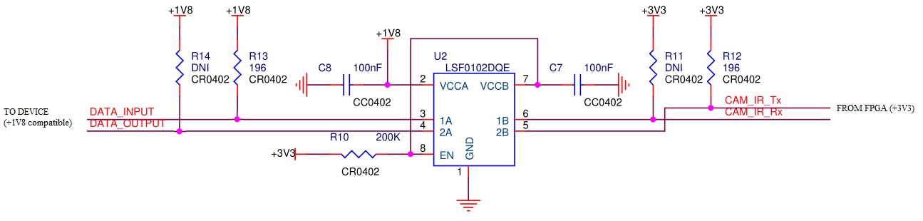
Other Parts Discussed in Thread: LSF0102

Hello,

I currently use a LSF0108 to perform +3.3V to/from +1.8V translation on a first board. Conversion is OK.

In some case, I need to cascade 2 LSF: connect first previous board (and so using first LSF +3.3V <-> +1.8V) to a second board (and so using a second LSF +1.5V <-> +3.3V).

Problem occurs in such situation: +1.8V -> +3.3V -> +1.5V.

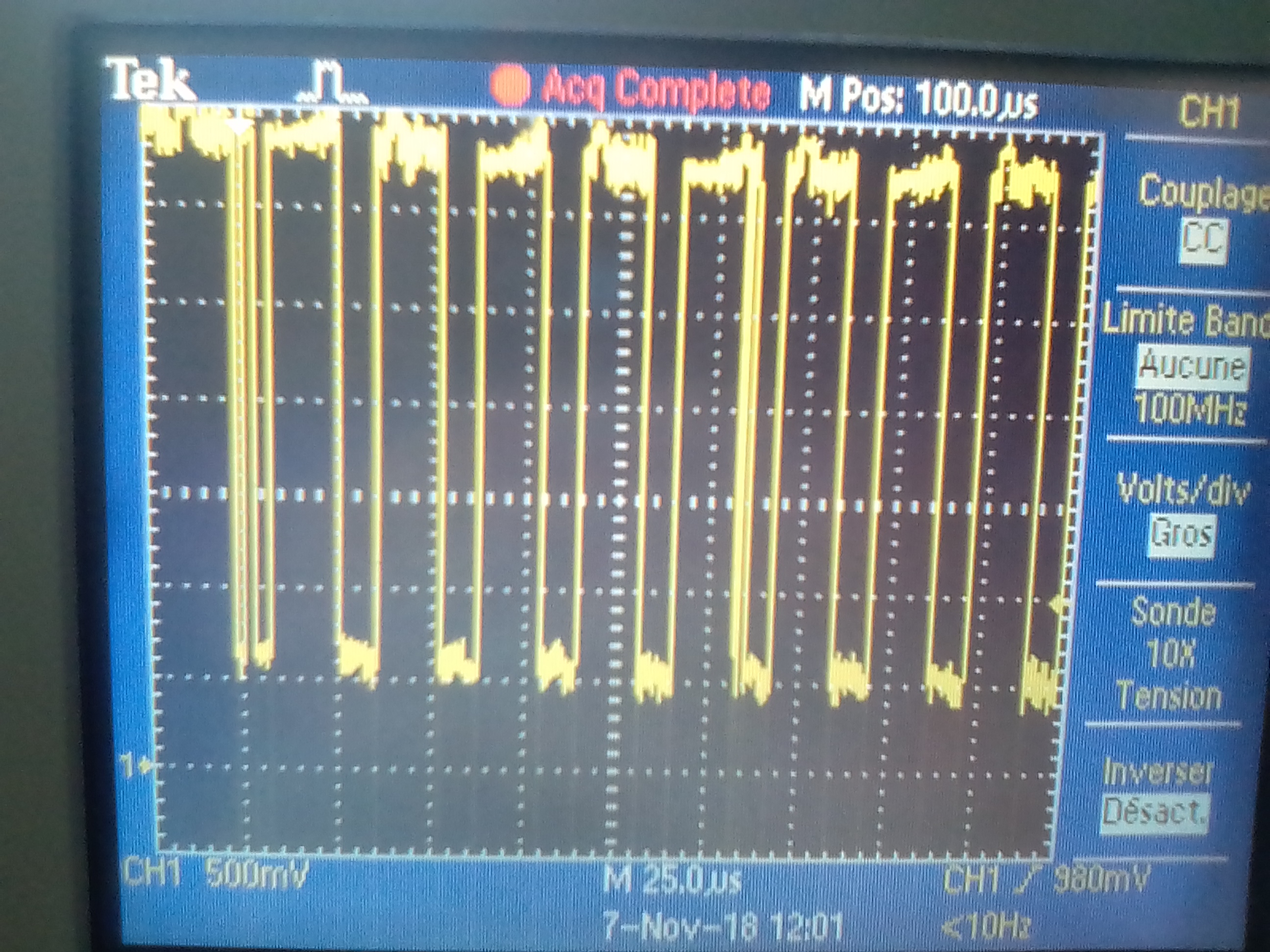
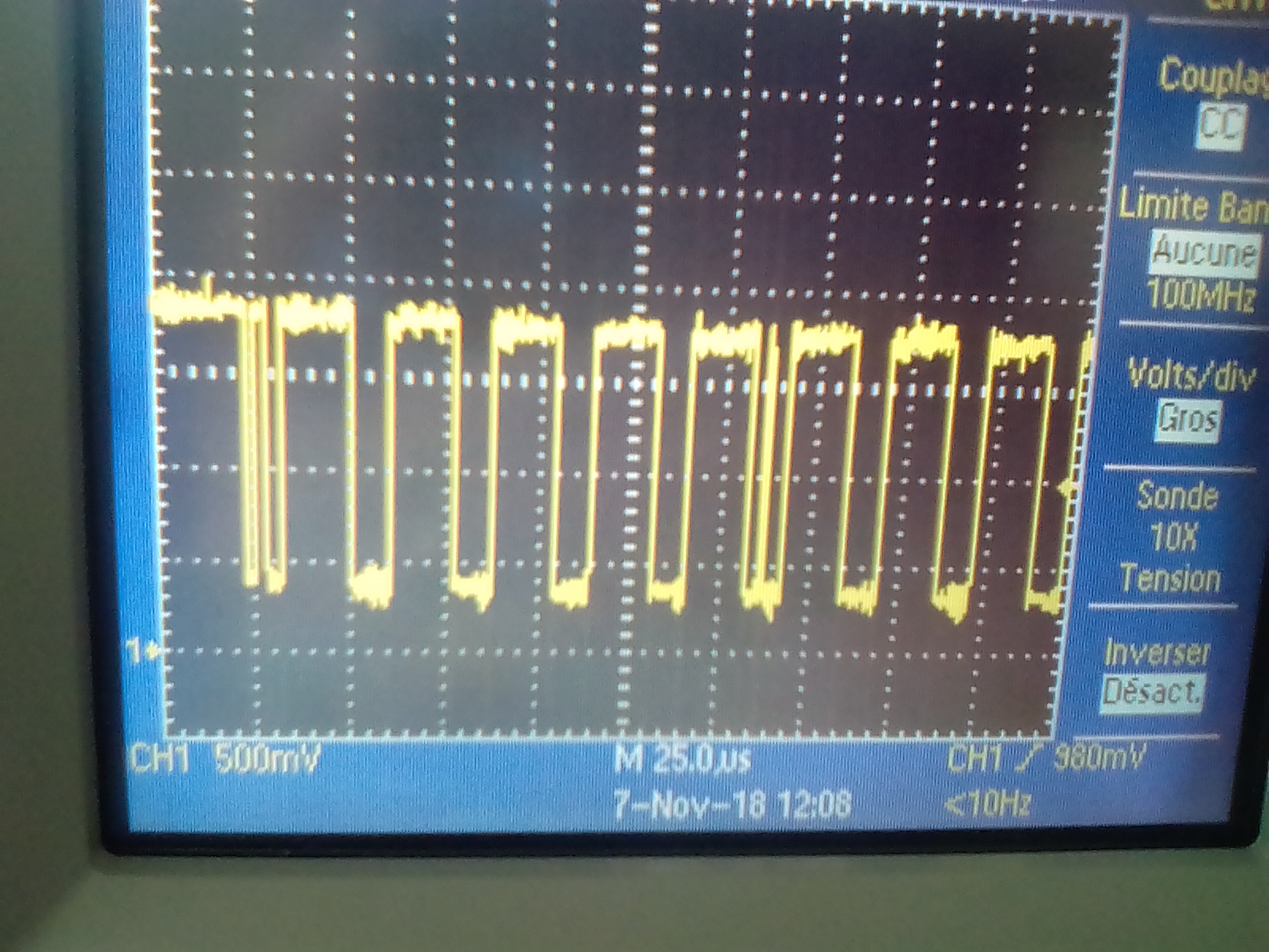
When my device at +1.8V logic outputs a logical zero, Ax signal (first LSF) is around 0.6V (I suppose it corresponds to the Vab voltage described in video 'Down translation with the LSF  family'). As voltage at Bx is slighty higher than Ax, Bx of first LSF is around 0.65V and again Ax of second LSF is around 0.7mV... which is higher than the Vil of my device (0.35x1.5V=0.525V) and so sampling data at +1.5V fails.

I am a bit confused with the 0.6V. Does it seem to be a bit too high? Is it a correct behaviour? How can we evaluate this Vab?

For information:

  • 'A' port of +1.8v->+3.3V has no pull-up
  • 'B' port of +1.8v->+3.3V has one pull-up (200ohms)
  • 'B' port of +3.3v->+1.5V corresponds to the same connection of previous (so same pull-up 200ohms)
  • 'A' port of +3.3v->+1.5V has no pull-up

May I need to have higher resistance to minimize sink current?

Many thanks.

  • Hi Sylvain,

    Could we get some schematics of the circuit? This will help us see what is going on.
  • Hey Sylvain,
    It sounds like the output driver is not strong enough to handle the current that is sinking into it. Can you increase the pull-up resistor values? This would reduce the current into your driver, and provide a lower "zero" for the first LSF.

    Also, when you say that the value of 0.7V is above your devices V_IL -- does that mean it's causing the device to switch or have problems? Typically a device will switch around Vcc/2, and you have a little more play than the recommended input low voltage.
  • Hi, 

    I merged the two boards... If there a problem if one LSF is at +3V3 while other is at +2V5?

    Note:

    R13 is required for module attached to DATA_INPUT/DATA_OUTPUT.

    My FPGA is at +1.5V. So the trouble with Vih...

    Thanks.

  • Thanks for your anwser.
    I'll try on my next day at work (!). I already changed to a bigger resistor without any change. I'll test with several values.
    FPGA has no particular problem except that it does not sampled data correctly (a '0' is often seen as a '1'). But yes I'll have a little more to play than the recommended voltage...
    Thanks.
  • Hi Sylvain,

    Were you able to test anymore resistor values? Just as Emrys suggested, I believe this to be an issue with the drive strength of the output driver.
  • Hi everybody,

    No... I changed with low resistor value (200ohms) and higher resistor values (up to 20k) with no significant better result.
    For the moment, the second board is not populated with the LSF0102 component (replaced by bypass resistors). It's not optimal (because I need to manage 2 different BOMs for 2 different projects) but it works...

    I'm waiting for a new board out of production so as to re-test in a cleaner environment.

    Thanks for your feedback,

    Sylvain.
  • Hi Sylvain,

    Got it, let me know how that testing goes. Feel free to save the scope shots and post them here as this will help us debug the issue with you if it continues.
  • Hi Sylvain,
    I see that you marked this issue as "not resolved" -- can you post additional details? We would be happy to help you resolve the issue.
  • Hi Emrys,

    Yes it is still confusing for me...

    I received a production lot of 4 boards. Only 2 boards are fully functionnals even if I use only one LSF (FPGA +3.3V -> LSF -> device compatible with +1V8), as represented in the below schematic:

    Note: R13 resistor is needed because of device requirement.

    For the 2 working boards, I've got the following scope shots. I represent the path 'CAM_IR_Tx to DATA_INPUT' (down translation) (sorry for the quality):

    • FPGA side:

    • Device side:

    -> Even if it is not perfect (is it possible to have a lower VOL level?), my device answers correctly.

    For the non-working board, I have:

    • FPGA side:

    • Device side:

    No visible activity

    I don't understand why the low level is around +1.25V (against +0.5V in the good board). And even if this is quite a high value, I see nothing on LSF output...

    May the boards be damaged?

    I change resistor R13 from 200ohms to 20k and 100k without any improvement.

    Thanks for your support!

  • Hi Sylvain,

    There are a few things I want to address here. First, is the signal path. You said it was CAM_IR_Tx to DATA_INPUT, but from your schematic it looks like it is supposed to be CAM_IR_Tx to DATA_OUTPUT. Can you confirm?

    The second thing is the drive capability of the FPGA. When driving low, it has to be able to sink about 17 mA due to R12. It seems like the FPGA is having a hard time doing this since the VOL values are pretty high. Changing R13 may not have an effect on the translation due to my first statement. I would increase the value of R12 to make it easier for your FPGA to drive Low closer to 0 V. This should help the pass through FET turn on.

    Also, to get a better understanding of how the LSF operates we have a great training series that you can watch. See link below to watch the video that covers down translation specifically:

  • Hi,

    Yes, you're right: I made a mistake in the schematics: it was CAM_IR_Rx (pin 6 of LSF) to DATA_INPUT. Sorry for this...

    So, for this down translation path (+3.3V to +1.8V), there is no resistor from FPGA side (R11 is DNI) and there is R13 from device side (because of external device constraint).

    I'll add R11 to see if it's better...

    Thanks.

  • Hi Sylvain,

    This could be the reason you don't see an output. If you continue to watch those videos, they will help you size the pull-ups to balance power consumption and data rate.