This thread has been locked.

If you have a related question, please click the "Ask a related question" button in the top right corner. The newly created question will be automatically linked to this question.

TXB0304: Simple circuit not functioning

Part Number: TXB0304

Hello to All,

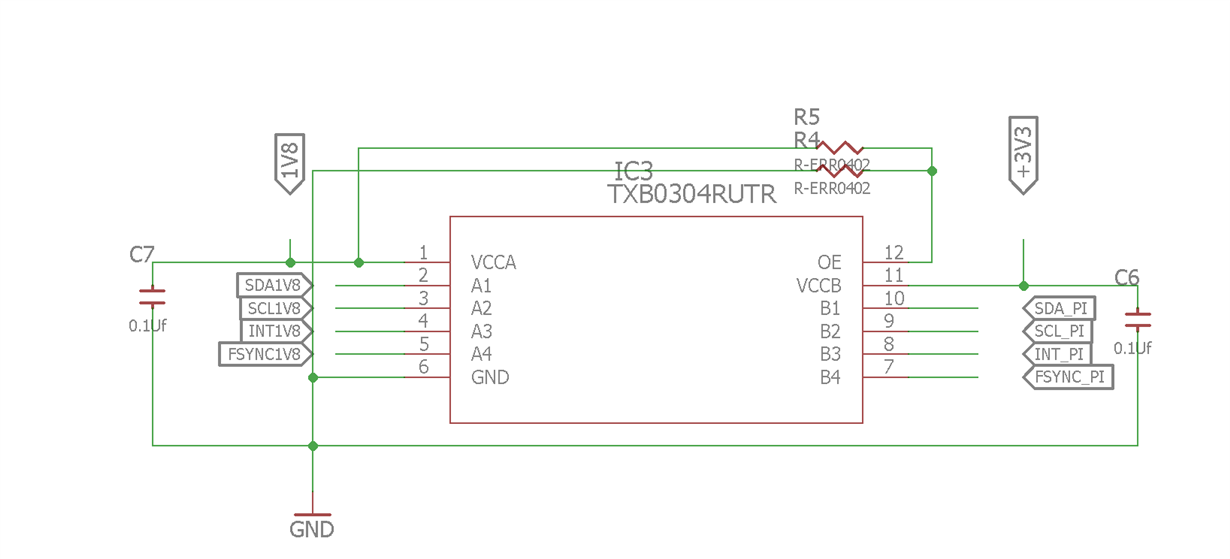
Thank you for taking time to consider my problem. I have set the TXB0304 as a level translator between a Raspberry pi zero W and an ICM20948, inertial sensor by TDK, formerly Invensense. The TXB0304 circuit is very simple in that it only has two capacitors in the circuit for bypassing both the VCCA and the VCCB. The signal lines are translated from one voltage to other, while the I2C lines out of the master, Pi, are present at the B "inputs" they do not appear at the "output" of A. The signal at the B ports looks as expected with an oscilloscope, but the scoped ports of A are without any indication that port B is toggling. The OE signal of the TXB0304RUTR has either a pullup or pulldown and have used both with a 4k7 ohm resistor but neither creates an enabled translator?

Thank you!

Cy Drollinger

  • Hi Cy,

    The TXB0304 is a buffered device with internal 1K series resistors on the IO ports. This, in addition to the external pullup resistors used for the I2C interface will create a voltage divider which will potentially fail translation.

    Please refer to the app note on the effects of pullup / pulldown resistors.

    Is there schematic and scopeshot available? Are there internal pullup/pulldown internal to the Rasperry Pi/ ICM sensor?

  • Thank you! As in figure 6. of the datasheet there are no pullup or downs. Your suggestion seems to indicate a failed translator due to undisired voltages that are voltage divided on account of the internal 1k resistors, but what if the circuit is as in the datasheet figure #6? Would you then be suggesting that the inputs and outputs of the systems needing translation are not of the push/pull configuration, internally to the chip? The oscilliscope indicates there is no sign of I2C activity at the 1.8V side, just nothing, despite having nice i2c signals on the 3.3V side. I think that the chip is not seated on the PCB or the circuit is not enabled?

  • There are no pullup / pulldown resistors within TXB and hence the question to you about any external pullup / pulldowns which will affect the signals.
    where is the 3.3V signal measured? Is it on the trace or on the device pin? and where is the 1.8V being measured, on the device pin or on a test point? For the TXB0304, the OE should be high to enable the IO ports, but from your statement you have tried both high/low but there is no output. you could measure the continuity by measuring on the multimeter between gnd and other pins about a presence of gnd diode.
  •  Sorry for the confusion, I have no pullups or pulldowns like in figure 6. of the datasheet. Both the 3.3V and the 1.8V are measured on the I/O lines or traces as the pins are a bit small to be measuring from. So, for the 1.8V the 1.8V measurement is taken on either the A1 or the A2 I/O trace and can be seen to approximately 1.8V. The 3.3V is measured on the B1 and or B2 trace and is approximately 3.3V. The i2c signal of either the SDA or the SCL is measured on the respective B1 or B2 and is the i2c master out of the Pi, and looks like an appropriate signal with digital data being deciphered into digital data that was sent from the Pi. The signal is not transferred to the A ports, however.

    Your link to the Power Sequencing for the AXC family is broken, is the powering sequencing tricky?

  • Thank you for pointing out the broken link on the app note. I have updated the link to rev A.

    OE connected directly to Vcca is fine without a pullup or pulldown resistor. I will assume that the R5 is installed and R4 is not.
    I do not see any issues with the schematic shown here.
    You have referred to issues with A1,A2 / B1, B2. However, is A3, A4 also having the same no signal issue as well?

    "So, for the 1.8V the 1.8V measurement is taken on either the A1 or the A2 I/O trace and can be seen to approximately 1.8V. The 3.3V is measured on the B1 and or B2 trace and is approximately 3.3V. "

    do you measure 1.8V DC on the A ports however, there is no digital signal coming out? I understand that meausring on the IO pins can be hard for QFN packages. This may also indicate a possibility that the soldering underneath may be shorted to the Vcca pin.
  • Cy,
    Is there any update? If not, I will close the thread for now and you can reply to it, which will notify me again and open the post.