This thread has been locked.

If you have a related question, please click the "Ask a related question" button in the top right corner. The newly created question will be automatically linked to this question.

SN74LVT8996: Part answers with RESET Code instead of the Address

Part Number: SN74LVT8996

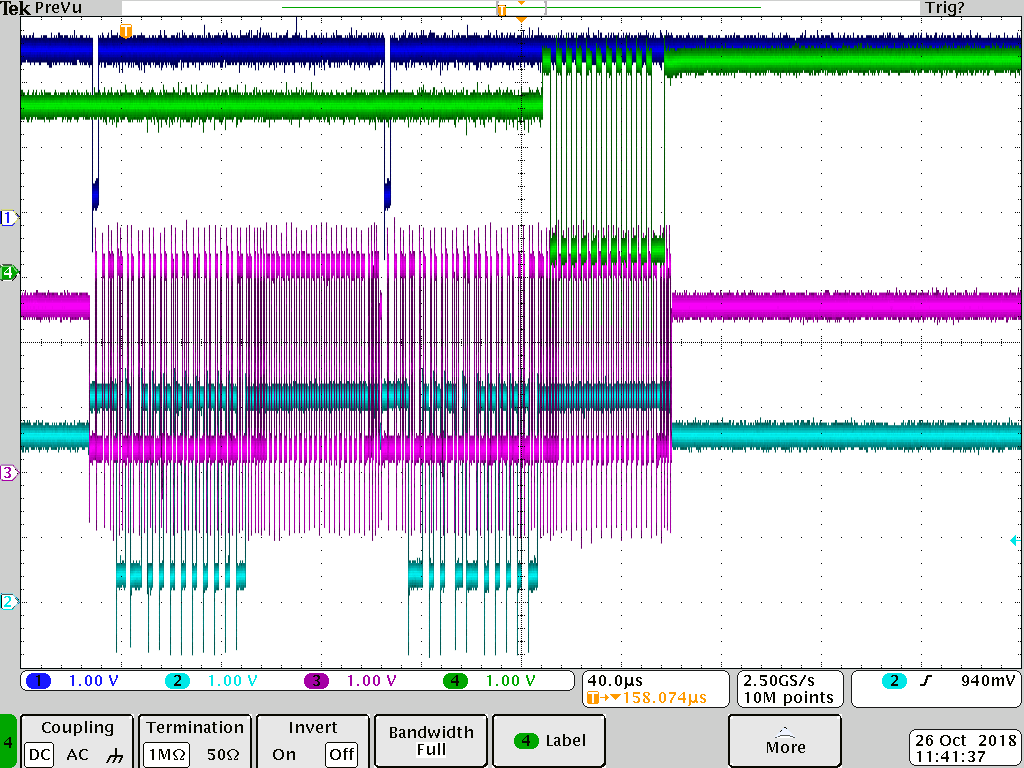
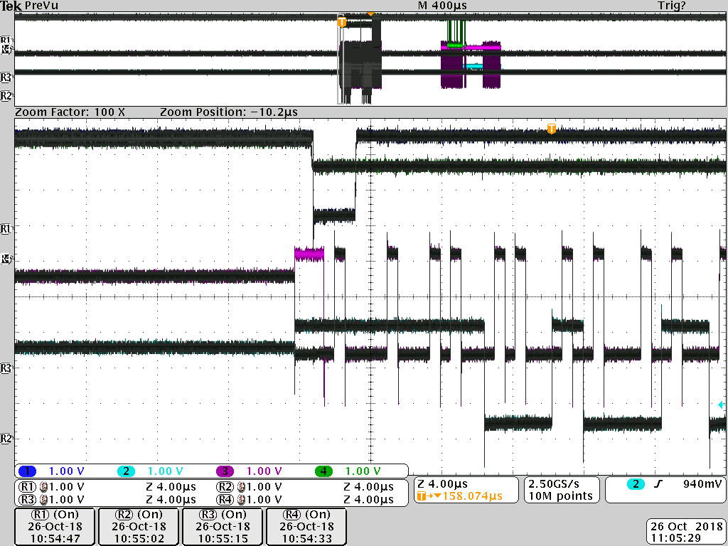
When I scan all the TAPs on my JTAG Bus, one of them answeres with  " I-S-10xZERO-S-I "

So far I know, this is the code for a Reset of the device. What can be the reason to induce the SN74LVT8996 to answer with this code instead of its address?

Sincerely, Steffen

  • Green    SDI (of the BusMaster)

    Blue       TRST

    Red        TCK

    Cyan      SDO

    ... on my oscilloscope picture...

  • Steffen,
    Your scope plot did not get posted properly.
    To post an image, use the "Insert Code, Attach Files and more..." link.
    Then use the paperclip to insert the file.

    Please provide more details on the topology and devices connected to your jtag chain(s).
    Please also define the signals with respect to the LVT8996, or include schematic.

    Regards,
    Wade
  • Unfortunately I have no better zoomed picture in the moment. This one shows the start of the communication. Do you need a better picture? The master changes data and clock separately. The slave sends the Data with the Clock edge.

  • Steffen,
    Unfortunately without more information I am not sure that I can help.
    I need to understand the topology of your JTAG solution. Is there more than one 8996, and only one responds with reset?
    Your signals probed do not match device pins, so I am uncertain what signals these represent relative to the device.
    A schematic would be helpful, along with better scope captures.
    Regards,
    Wade
  • Hello,

    On our Bus system with a double sided, 21 Position Backplane the problem occured at the Card in the middle of the Bus direct opposite of the JTAG bus master.

    On the Backplane are Bus termination resistors, on both ends of the Backplane 220 Ohm against P3.3V, 1 kOhm against GND, resulting in 110 and 500 Ohm.

    I measured reflections on the TCK slopes (on the other signals, too)

    In the middle of the Bus signal reflections from both sides added in a unfortunately manner and the Logic levels have been reached, I think.

    So the one JTAG Bus slave received more clock impulses.

    Withe the capacity of the Oscilloscope probe the slopes bekame somehow flatter and the effect has gone...

    Thank you for your support!

    Steffen