This thread has been locked.

If you have a related question, please click the "Ask a related question" button in the top right corner. The newly created question will be automatically linked to this question.

LSF0204: LSF0204 Voltage level stabilization

Part Number: LSF0204

Hello,

I am using a LSF0204 with two signals, one clock and one data.

I am doing a down translation for the clock and a bidirectional translation for the data.

i translate between 3.3v and 1.8v @ 1MHz.

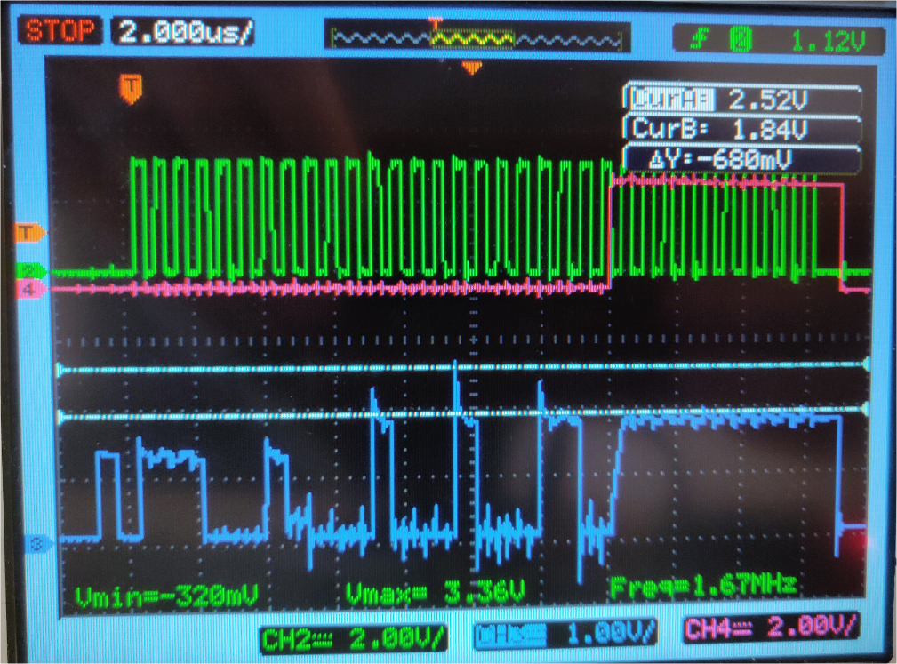
Here is a scope capture (sorry for the poor ground connection...) but my problem is that the data in blue is something like clamped at the beginning of the frame.

Except the beginning, the translation is well done.

I have pull-up resistor on each side of LSF on data line.

I tried different values without improvement.

BR

  • Hi Nicolas,
    Can you provide a schematic and a cleaner scope shot of the data? I'd like to get a closer look (ie faster time scale, smaller voltage scale)

    Also, do you know which device is driving during each time period shown?
  • Hi, 

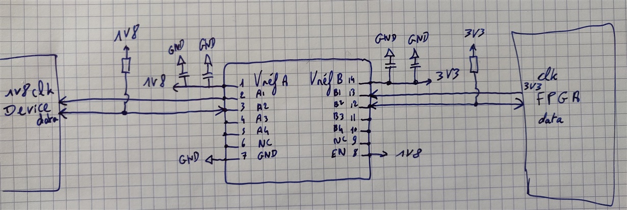
    Yes here is a schematic:

    Clock line is only down translated from 3v3 to 1v8

    Data line is bidirectionally translated 3v3<->1v8

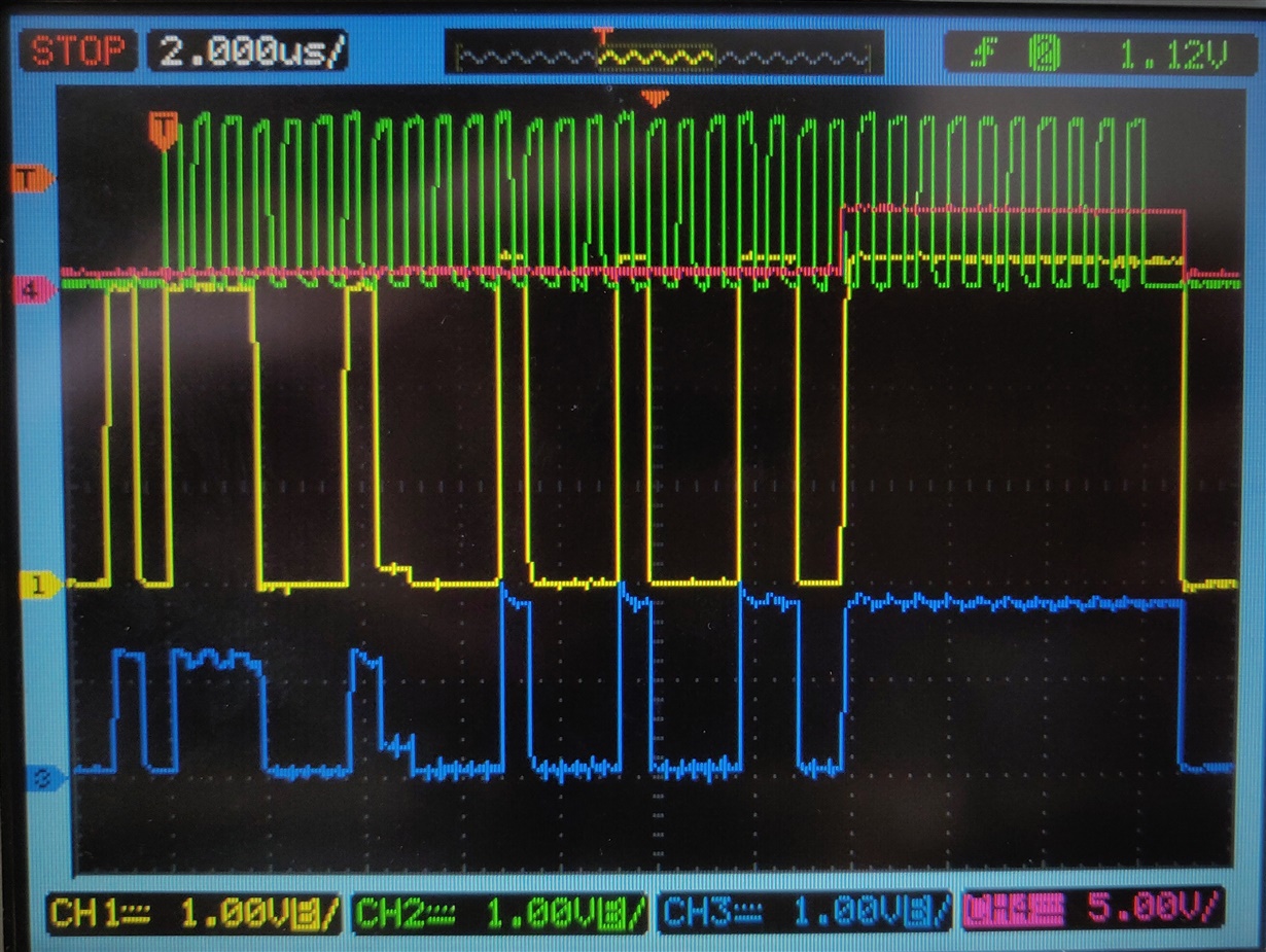
    Here is a scope screen capture:

    Green: clock at device pin

    Yellow: data high side (fpga side)

    Blue: data low side (device side)

    Pink: this signal is here only for information, it represent the fpga tristate control bit. when 0 the fpga drive the line, when 1 the device drive the line

    Here when the tristate bit is set, the device does not drive the line because it does not detect the frame due to a low voltage at the frame beginning.

    So i don't understand why, but at the frame beginning, FPGA drive the data line and the voltage is a little bit low in high side, which apparently affect the low side.

  • I would recommend watching the videos on the LSF family of translators.  In particular, "Up Translation with the LSF Family" gives some very helpful details.

    If you watch from ~2:12, you can see how the output waveform curves up to Vcc.  This is caused by the passive nature of the LSF family of translators.  The parasitic capacitance on the line and the added pull-up resistor create an RC circuit that takes time to charge.

    Since your circuit was in the 'low' state prior to going into high-impedance mode, the line voltage slowly rises as per the RC transient response curve.

    As for the first part of the curve, it looks to me like something is causing the line to be 'dragged down.'  The LSF0204 is extremely simple internally -- just an nMOS based switch and some bias/enable circuitry.

    I see that the yellow signal is also a bit lower in the first 8us... what kind of load is this signal driving? Just based on the above scope shot, I think it's fairly large (maybe 10+ mA?).  In this case, it wouldn't be surprising to see a much lower "high" voltage due to the voltage drop on the pull-up resistor.