This thread has been locked.

If you have a related question, please click the "Ask a related question" button in the top right corner. The newly created question will be automatically linked to this question.

CD74HC4050: The usage question due to mismatch of spec. and measurement result

Part Number: CD74HC4050

Hi All:

I am using CD74HC4050 on my design.

When i measure CD74HC4050 VIL ( VCC: 3.3V).

I found following things:

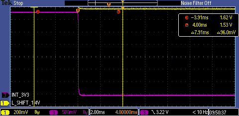
1. Input voltage under 1.4V,  CD74HC4050  output 0V (Fig.1)

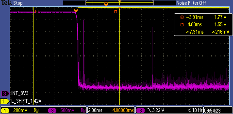
2.  Input voltage between 1.415V to 1.425V,  CD74HC4050  output unstable waveform (Fig.2)

My questions are:

1. From datasheet, there have no VIL value(max) operated at VCC 3.3V, can i use interpolation method to acquire this value ?

2. If i use interpolation method, the calculated VIL(max) is about 0.93V. This value is high difference of my measurement result 1.4V, why ??

3. Spec. mentioned this part have High Noise Immunity: NIL:30%, NIH:30% of VCC at VCC =5V. What does this mean? It means CD74HC4050 has schmitt trigger buffer or ??

Thanks

Jimmy

Fig1

Fig2

  • Hello,

    This device does not have Schmitt Trigger inputs. I believe you are misunderstanding what is meant by VIL. Here is an FAQ that explains the VIH and VIL specs in the datasheet.

    [FAQ] Why does my device not switch at VIH or VIL?

    Thanks!

    -Karan

  • Dear Sir:

    From my understanding, the VIL (max) is that no matter which CD74HC4050 i choose to do experiment.

    If i control input voltage below VIL(max), i can ensure CD74HC4050 output low.

    I was just a little curious that  i measured about 5 samples and the switching voltage range were all between 1.41~1.43V.

    What's the distribution of the switching voltage versus quantity ? 

    And could you help to explain what's the meaning of following items mentioned in spec. ?  

    3. Spec. mentioned this part have High Noise Immunity: NIL:30%, NIH:30% of VCC at VCC =5V. What does this mean (because there have no schmitt trigger in 4050 design )? 

    Thanks.

    Jimmy

  • Hi Jimmy,

    Just to confirm, CMOS devices do not switch at VIL and VIH. They switch at threshold voltages of VCC/2.

    VIL(max) for this device at 3.3V will be around .94V if you linearly interpolate the values on the datasheet for the VIL(max) at Vcc = 4.5V and Vcc = 2V.

    So staying under .94V will confirm that the signal is a guaranteed low. 

    As for switching at 1.4V ~ 1.43V seems great since as mentioned in the FAQ post I gave in my previous response the device is supposed to switch at around Vcc/2. 

    It also mentions that you should never be operating in this region due to the massive current draw and damage this will cause to the device.

    As for the NIL and NIH specs, they are basically VIH and VIL min and max regions. You can learn more about them here if you look for noise margins:

    Thanks!

    -Karan