This thread has been locked.

If you have a related question, please click the "Ask a related question" button in the top right corner. The newly created question will be automatically linked to this question.

looking for conversion of clipped sine wave to square wave conversion

Other Parts Discussed in Thread: SN74LVC1G17, TLV3201, SN74LVC1GX04, TLV3501

Hi Team

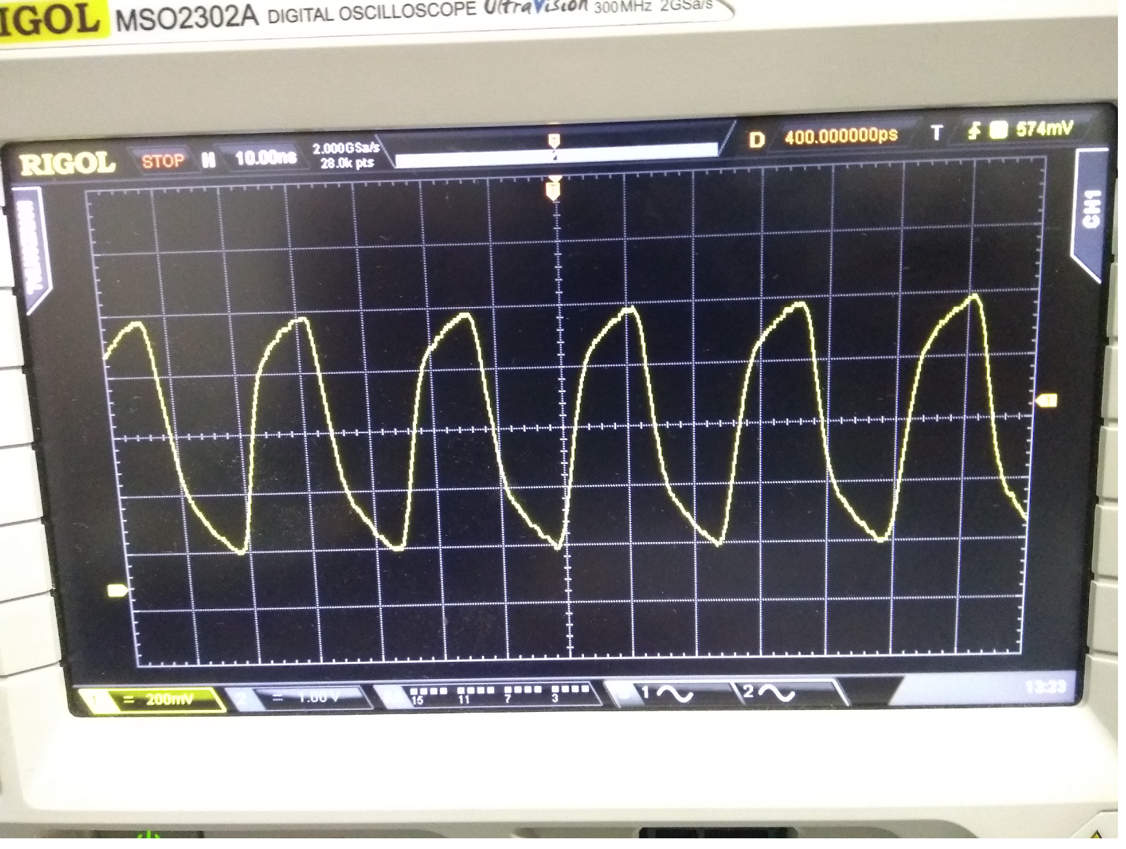
I need one Part number which can convert the clipped sine wave  ( 1MHz and 10 Mhz ) (0.7pk to pk) to Square wave (5V) .

Regards

Nitesh

  • "Clipped" would imply that the signal goes from rail to rail, but then it would not be 0.7 V peak-to-peak.

    If the signal were guaranteed to go both below and above the low and high input thresholds, you could use a Schmitt-trigger buffer. With something like the SN74LVC1G17, this would require a swing of at least about 1.5 V. (And if the input signal is not symmetrical about the threshold, the output does not have a 50 % pulse width.)

    With such a small amplitude, you have to use a comparator (e.g., TLV3201).

  • Hey Nitesh,

    In addition to what Clemens suggested, I think you could use an SN74LVC1GX04 to accomplish this.  This device is usually used to drive a crystal oscillator, and the output of most crystals is a fairly small sine wave (0.5 to 1V in my experience).

    The input needs to be AC coupled (add a series capacitor, 0.1uF should work well), then connect directly to the X1 input. Add a feedback resistor from X2 to X1 to provide the appropriate bias -- 100k to 1M should work well.

    Then your output shows up at Y.

    You may have to tweak some passive values, but the circuit is relatively simple and only requires one ic.

  • Nitesh

    Please provide a picture of the waveform that you want to convert to 5v. Ideally this would be an oscilloscope screen shot so everyone can see the common mode voltage level and signal swing. From your original post it sounds like the amplitude is 0.7v pk-pk but it’s best to confirm with a picture.

    From that information we can determine if using a logic gate or a comparator makes sense. If a comparator is best suited, the tlv3201 should be looked at first. If that’s not fast enough, the tlv3501 would certainly work. But let’s hold off on going down this path until you attach a waveform.

    Chuck

  • Hi Clemens

    I will try simulating TLV3201 and share the result.

    Regards
    Nitesh

  •  Hi Chuck

    Thanks for the reply.

    Can you please check and suggest me if i can go with TLV3201

    Regards

    nitesh

  • Nitesh

    this waveform is a bit faster, more like 40MHz, so you will need to go with the TLV3501.  The propagation delay of the TLV3501 is less than 10ns, so this will be required to handle this higher frequency.  The TLV3201 has a prop delay of 40ns, so I can't recommend that device for this higher speed.

    Chuck

  •  Hi Chuck

    Thanks for the reply.

    I have simulated the same with TLV3501 .But i am not able to get the I/P waveform with 0.8V Pk to Pk.

    In my waveform you can see that i have set VIN as 0.8V but waveform is reflecting as 2V.

    Can you please check my simulation result let me know what is to be updated.

    BR/Nitesh

  • Can you please include the attachment to your TINA simulation file?

    Thanks,
    Jonny
  • Hi Jonny

    PFA simulation file here.

    Regards

    NiteshTLV3501.TSC

  • Nitesh,

    It seems that you actually adjusted the DC offset value of the input waveform, not the amplitude. To fix your Vin to be 800mV:

    1. Double click on VIN
    2. Adjust DC Level [V] to 0V
    3. Click "Sine Wave" and the "..." button next to it
    4. Change the amplitude to 400m to set 0.8V pk-pk

    If this answers your problem, please click the "This resolved my Issue button" so that I may close this thread.

    Best Regards,
    Jonny
  • Hi Jonny

    Thanks for the reply. It works

    What could be the reason for having Negative pulse is less time period as compared to positive pulse.

    Is it so i need to change the discrete to map it equally.Can you please check and let me know.

    I am attaching the waveform as well as simulation file for the reference.

    Regards

    Nitesh

  • Hi Nitesh,

    The reason why the rise/fall times aren't symmetrical is due to the feedback resistor R3 in your circuit.

    Although the datasheet defines the typ Trise/Tfall = 1.5ns (typ), the hysteresis implemented in your circuit will cause some changes in the rise time and fall time as well as propagation delay of the device.

    Regards,
    Jonny