This thread has been locked.

If you have a related question, please click the "Ask a related question" button in the top right corner. The newly created question will be automatically linked to this question.

LSF0108: LSF0108 Leakage & power on sequence design questions

Part Number: LSF0108

Hi Sir,

Please help me clarify, Thanks

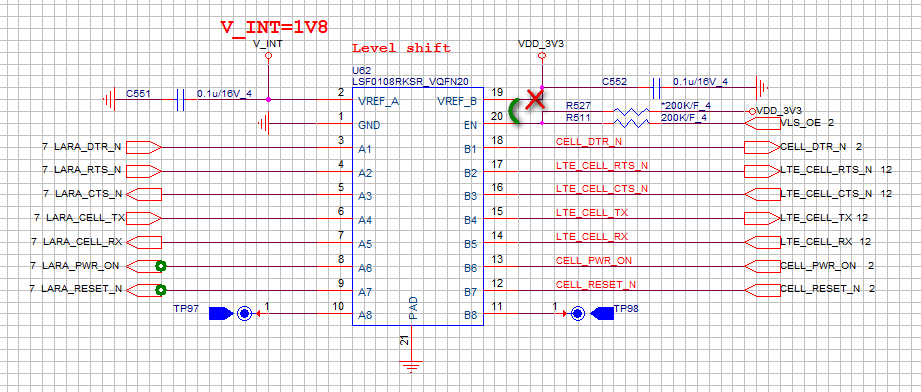
1. As the pic shown as below, Vref_B is determined by Vref_A + Vth. LSF01 seems have power sequence right? Vref_A should power up before Verf_B right?
2. I did some rework, power up Vref_A 1.8V first and I can get 2.6V on Verf_B. Port B signal level still are 3.2V. But why port A signal is 2.0V not 1.8V? should we add pull-up resistor to 1.8V on port_A?
3. In our currently design, VDD_3V3(actually 3.2V) power up before V_INT, I think that’s why we can get 2.4V on Vref_A, correct?
 

  • Hi Anne,

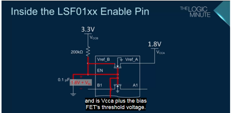
    With the right connection as shown in the video with VrefB/ EN connected through the 200k bias resistor to 3.3V, VrefA at 1.8V, the gate voltage will be approximately be VrefA + Vt. So, 2.6V at the EN/VrefB pin looks right to me ( 1.8 + 0.8V = 2.6V).

    From the schematic you have shown, the VrefB and EN has not been connected right. but I assume that the connection in the board is set right with the modifications you have shown.

    For translation, having the pullup resistor to the appropriate pullup voltage is ideal.

    As you can see here, the Vbias node voltage(VrefB and EN pin) reads ~2.6V.

  • Hi Shreyas,

    Thanks for your details reply, and one more question about the supply sequence of Vref & VrefB?

    Is there any limit that Vref_A should power up before Verf_B?

    And it is must add pull up resistor on A1 & B1, correct?

    Thanks

  • Anne,

    There is no particular sequencing required for this device.

    Mostly yes. If you have a push pull signal, the input side wont require pullup resistor.