Dear team,
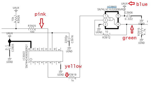
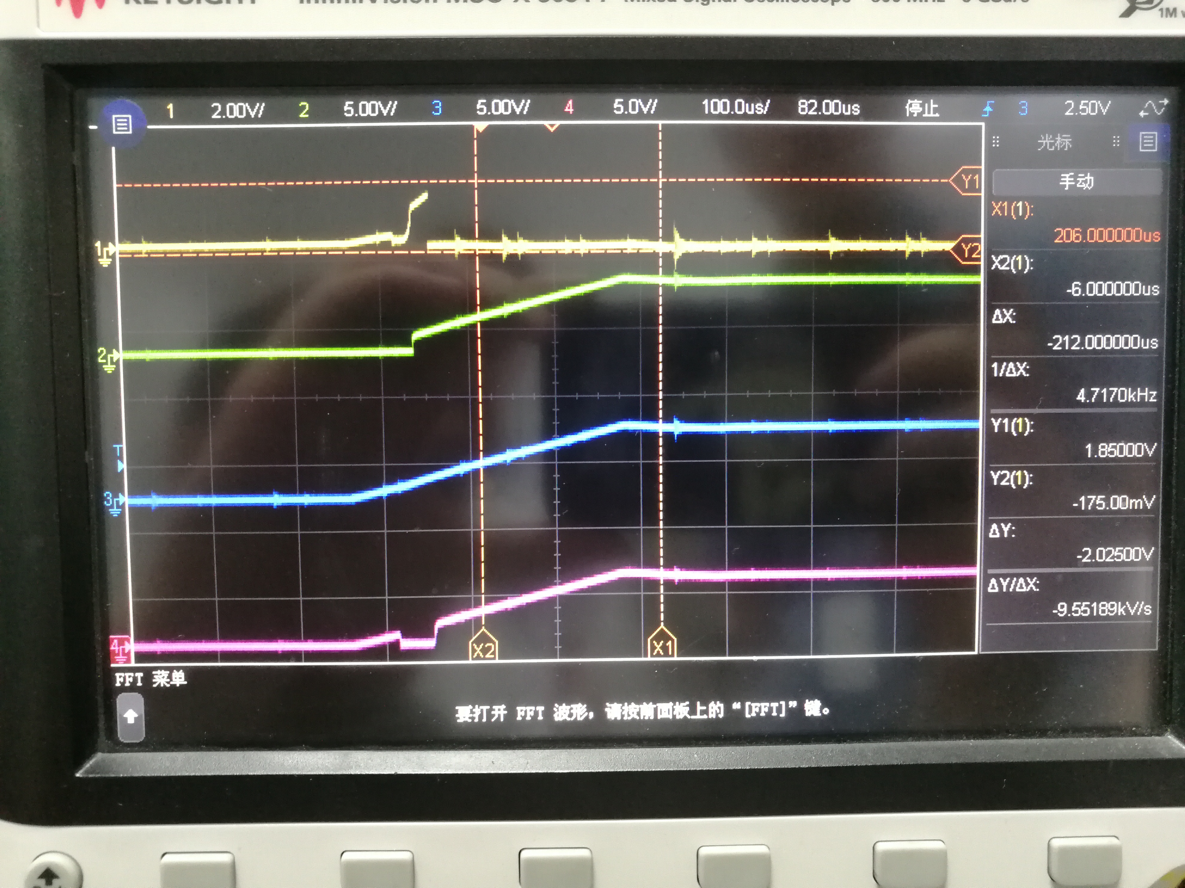
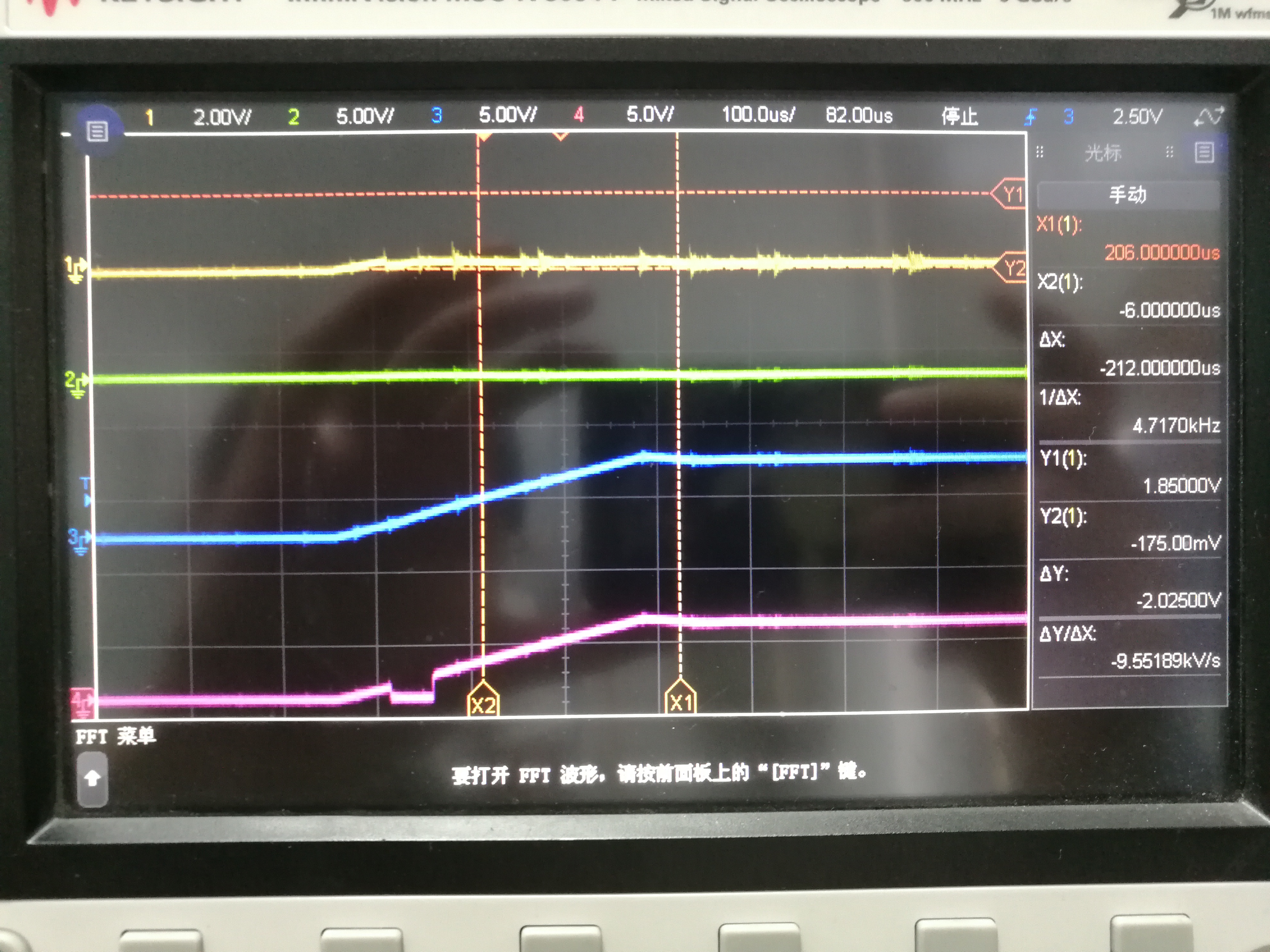
The following problems were found during the test.(Yellow: power, Green: 4 pin, Blue: 5 pin, Pink: 7 pin)

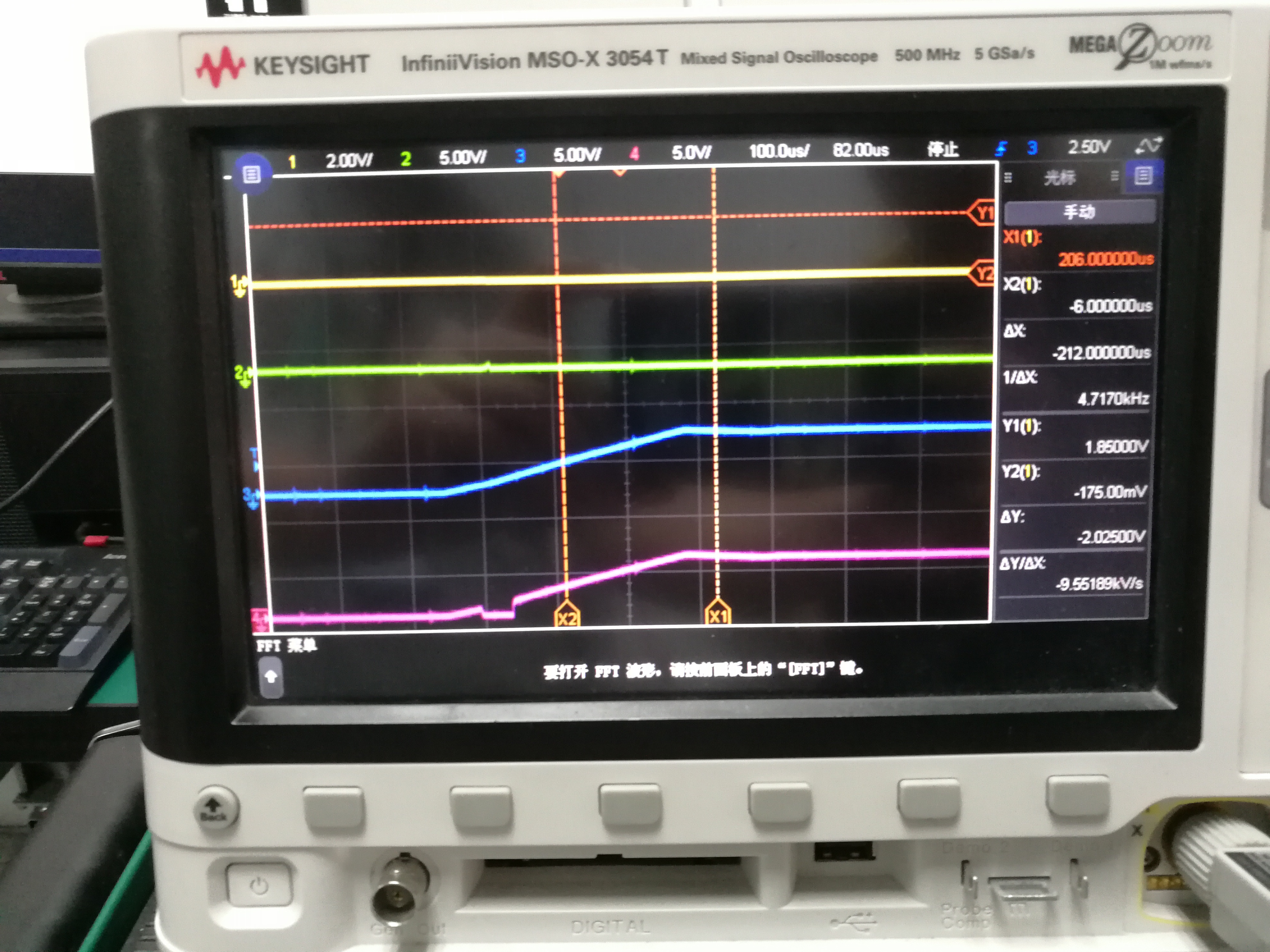
1.When the temperature is -40 °C, the low-voltage power-on and power-off test is performed.
> When the power is off after a long time (about 20s or longer) and then power on, the measured waveform is shown in Figure 1. No collision will be reported.
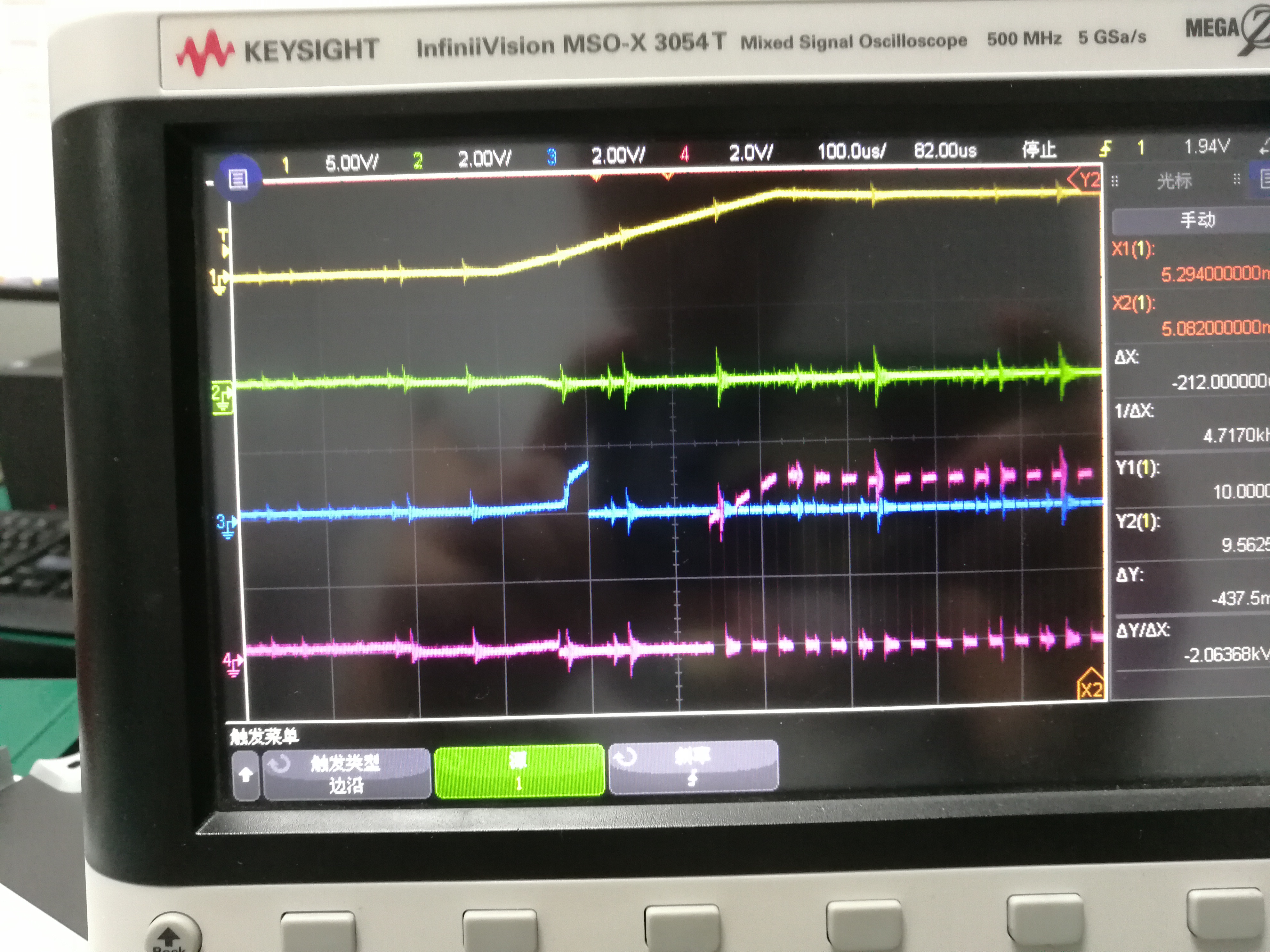
> When the power-off time is short (at this time power supply voltage has reduced to 0) and then power on, the measured waveform is shown in Figure 2. When the collision fault is reported, you can see that the input of the device has a spike and the voltage is about 1.6V - 1.8V, the output of the device is high, as shown in Figure 2;

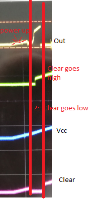
2. When the temperature is adjusted to 25 ° C, the test waveform is shown in Figure 3.