This thread has been locked.

If you have a related question, please click the "Ask a related question" button in the top right corner. The newly created question will be automatically linked to this question.

Decoupling capacitors: contradicting TI guidelines?

Hello,

I have a question regarding the layout of a 4-layer microcontroller board. The board includes a 100 MHz microcontroller, a couple of Sigma-Delta-AD converters (16 bit, 16 SPS) and some little logic devices. I think the latter are generating the highest frequencies on the board (the signal clock speed is low frequency, e.g., 100 kHz, but the edge speed of LVC devices are in the 5 ns range). So I would not call the layout "demanding" with regard to "high speed".

I was looking for best practices on placing  routing  decoupling capacitors and got confused by obviously contradicting guidelines.

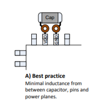
For example the http://www.ti.com/lit/an/spma056/spma056.pdf "System Design Guidelines for the TM4C129x Family of Tiva™ C Series Microcontrollers" recommend this placement  routing option as best practice on page 20:

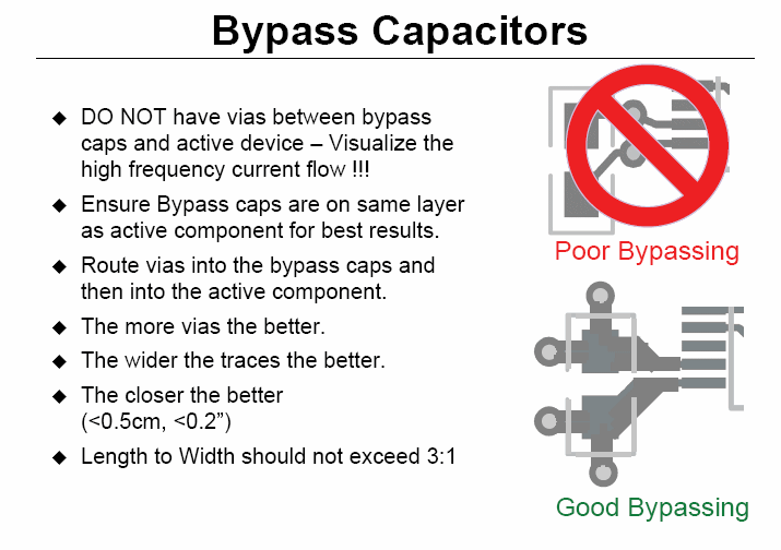
However, the following TI powerpoint http://www.ti.com/lit/ml/slyp173/slyp173.pdf on "high speed design" seems to reject exactly this "best practice" on page 5-23:

I know that the issue of decoupling capacitors is open to discussion, i.e., looking at sources external to TI, one finds even more differing suggestions, e.g., http://www.sigcon.com/Pubs/news/9_07.htm

I understand that when it comes to high speed design (> 1 GHz), one will have to apply simulations to the individual layout to "do it right", however, in the domain of low speed design (< 100 MHz) I expected to find a consensus on "best practices", at least in the TI realm. This seems not to be the case.

I'm a little confused. Please advise. Thanks.

  • Figure 18 of the TM4C129x Guidelines is not about placement, but routing. And TM4Cs are not quite as high speed.

    The Signal Consulting article talks about a case where the distance between the capacitor and the IC is larger than the PCB thickness, i.e., where the trace length becomes noticeable compared to the length of the vias. (If the inductance of the two vias is larger than that of the trace, going through the ground plance is worse.)

    The recommendation in SLYP173 does not really contradict the other ones. Use it. (Having more vias is probably overkill in your case; you're likely to drop them when you run out of space …)

  • Hi Clemens,

    Thank you for commenting.

    Clemens Ladisch said:

    Figure 18 of the TM4C129x Guidelines is not about placement, but routing. And TM4Cs are not quite as high speed.

    Sorry for my bad wording. I corrected the original posting. So what is "high speed"? What was high speed 20 years ago probably will not be considered high speed today. I assume that microcontrollers in the 100 - 200 MHz range do not count as high speed devices. 

    Clemens Ladisch said:

    The Signal Consulting article talks about a case where the distance between the capacitor and the IC is larger than the PCB thickness, i.e., where the trace length becomes noticeable compared to the length of the vias. (If the inductance of the two vias is larger than that of the trace, going through the ground plance is worse.)

    I didn't catch this trace length to pcb thickness discussion. I assume that the Signal Consulting article's suggestions are especially advantageous for thin PCBs, i.e., PCBs where the Vcc and ground layer are close enough to form a capacitor of noticeable capacity so that this capacity is supplying the IC with charge directly.

    Clemens Ladisch said:

    The recommendation in SLYP173 does not really contradict the other ones. Use it. (Having more vias is probably overkill in your case; you're likely to drop them when you run out of space …)

    SLYP173 requires that I should "not have vias between bypass caps and active device" while the TM4C129x Guidelines places vias between caps and device. How is this not contradicting? 
  • The TM4C129x Guidelines want to tell you only that you should use short traces. While the image shows vias between the caps and the device, it does not forbid you from placing the cap between vias and device.

  • Clemens Ladisch said:

    The TM4C129x Guidelines want to tell you only that you should use short traces. While the image shows vias between the caps and the device, it does not forbid you from placing the cap between vias and device.

    Thanks, your clarification is helpful.
    However what's really causing my confusion is that the notes on "high speed design" (SLYP173) explicitly advise against placing vias between bypass caps and the device.
    So - I guess the design hints in SLYP173 are relevant to designs that handle speeds and edge rates of > 1GHz.