This thread has been locked.

If you have a related question, please click the "Ask a related question" button in the top right corner. The newly created question will be automatically linked to this question.

SN74AVC4T245: Why would the part use excess current

Part Number: SN74AVC4T245
Other Parts Discussed in Thread: SN74AXC4T245, SN74AVCH4T245, TXB0104

Hello team,

Hope you are doing well and staying safe. When you get a chance please provide feedback on below from customer:

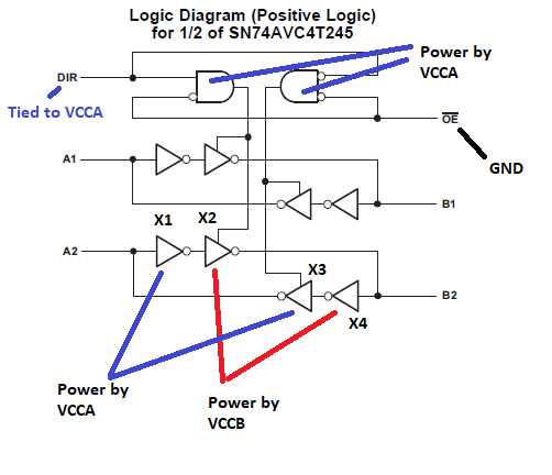
We are using SN74AVC4T245 (SN74AVC4T245RGYR) in our design and the contract manufacturer has reported a number of cases where the board is using elevated current. It seems that they have traced this back to this component.  Replacement of this component clears the excess current issue and putting the replaced component onto a known good board causes that board to exhibit the same excess current. My understanding is that they have taken 197 samples from the reel and applied 3VDC from pin16 VCCB to pin8 GND and found that 25 of them are drawing >4mA of current which is orders of magnitude larger than I would have expected. The state of the IC in our application when we are concerned about quiescent current is when VCCB is 3VDC and VCCA is off.  Unless I’m missing something the total draw in this situation should be microAmps.  I don’t think there is any residual voltage on VCCA but would be cause elevated current?

Also is the test the contract manufacture performed valid or should they connect the ground reference to both pins 8 and 9?  Could floating IO lines be a cause for this?

“A side” is normally powered 1.8V 100nF, “B side” normally 3V 10uF

B is on whenever A is on

A and B are sometimes both off

A turns on subsequent to B turning on; A turns off before B turns off

“A side” connects to a cellular module, “B side” connects to an MCU

VCCA has a 100k pulldown in addition to the discharge through the powered-down cellular module. 

Connecting the /OE pins to anything other than ground is not going to be something we can cut into production very easily.  I interpreted that if one supply was not powered, the inputs would be Hi-Z

Here is a snippet of the application circuit:

  • Hi Randhir,

    Doing well and staying out of trouble as much as possible.

    As you have suggested here in the query, the IO lines must be held at a known voltage level and not be left floating.

    You could consider switching over to SN74AXC4T245 which mitigates this issue of floating io pins and limits excessive Icc current consumption during the power off condition on one of the supplies.

    You could also try having pulldown resistors on the B ports to see if the current goes down.

    Also, to confirm, there is normal current consumption during typical operating condition ( both supplies active) correct?

  • Thanks Shreyas. Is this device p2p compatible?

  • We dont have RGY package of sn74AXC4T245 unfortunately, but the PW and RSV packages are P2P with AVC.

  • Shreyas,

    Below is customer feedback:

    My understanding is that current consumption is normal when both supplies are on. 

    The part you have suggested does not seem to have a RGYR package which we are using.  Would the SN74AVCH4T245 that Barrett suggested be acceptable? Having read the app note SBA004, could you please clarify if my statements below are accurate:

    In our application, the corner case of note is when VCCB is on and VCCA is off.  I infer that the internal gates appear as follows:

    • X1 powered off
    • X2 powered on, disabled
    • X3 powered off, disabled
    • X4 powered on
    • A2 is connected to a powered down device externally and X3 is output is powered down.  A2 should be 0V, clamped to 0.7V through protection diodes to VCCA (off)
    • X2 input should be 0V as X1 is powered down
    • B2 is connected to an IO pin externally which is configured to Input.  No external pullup or pulldown.  X2 is disabled and should not influence B2
    • Float on B2 could cause shoot-through/oscillation on the output of X4 

    If so, a pulldown on B2 (and B1) should help right?

    Also if this is the case, SN74AVCH4T245 would have the same problem without pulldowns on B1 and B2?


  • Randhir,

    The block diagram is a simplified version of the internal structure and not an actual internal circuit.

    Having the bus hold circuits wouldnt recommend having external pullup or pulldown resistors. however, bushold circuits have the feature to hold the last known state through weak feedback latch whenever the IO ports are left floating.

    I would suggest considering to move to SN74AXC4T245 if its possible to eliminate this, or have pulldown resistors on the B ports( active power supply ports)

  • Shreyas,

    See below:

    Thanks for the advice. Since the 2DIR IO is referenced to VCCA and is pulled up to VCCA, do you suppose it would have been better to make VCCA side the MCU side and VCCB the Cell side?  (MCU is never off when the cell is on). That way the direction ports would be controlled whenever the MCU is on and the cell is off. Sounds like that would matter for the AXC version but might it have helped on the AVC (assuming pin 6 and 7 are being pulled down to ground)?

    I know the TXB0104 has a restriction that one supply has to be the larger one.  I do not seem to see that sort of restriction on this part.

  • Hi Randhir,

    It is true that there is no restriction on the Vcca and Vccb supplies like the TXB.

    The supplies of the AXC and AVC and fully configurable across the operating voltage of 1.2 <>3.6 ( 0.65 <> 3.6V for the AXC).

    With that said, you could have the Vcca to the MCU as this is never off and the DIR pins will always have a reference voltage.