• Join
  • Sign In with my.TI Login
Texas Instruments
  • Products
  • Applications
  • Tools & Software
  • Support & Community
  • Sample & Buy
  • About TI
Sample & Purchase Cart Sample & Purchase Cart
  • Search
  • Advanced
TI E2E™ Community
  • Support Forums
  • Blogs
  • Groups
  • Videos
  • 简体中文
  • More ...
TI Home » TI E2E Community » Support Forums » Low Power RF & Wireless Connectivity » Low Power RF Hardware & Tools Forum » matching network & layout for cc1101-q1
Share
Low Power RF & Wireless Connectivity
  • Forums
  • Announcements
  • Files
  • E2E Wiki
Options
  • Subscribe via RSS

matching network & layout for cc1101-q1

matching network & layout for cc1101-q1

This question is answered
Mir
Posted by Mir
on Nov 25 2012 16:39 PM
Prodigy150 points
411351553_MLRF0805.pdf

Hi,

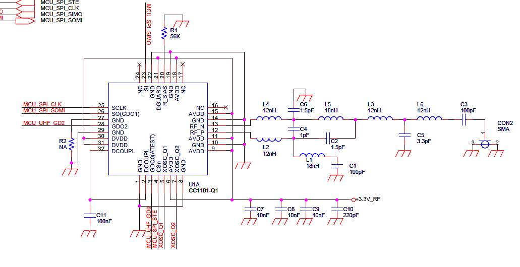
1. cc1101-q1 has a different footprint from the regular cc1101 - So does the layout of the reference design need to be modified to suit the -q1 part?

2. Also, handling 0402 components is extremely difficult. A 0805 inductor with >1GHz SRF is attached. can this be used for the matching network?

3. Similarly, please suggest 0805 type capacitors which can match with your circuit.

Thanks in advance,

Regards

Report Abuse
  • Reply
You have posted to a forum that requires a moderator to approve posts before they are publicly available.
All Replies
  • Mir
    Posted by Mir
    on Nov 26 2012 04:08 AM
    Prodigy150 points

    Hi,

    A follow-up query.

    The reference design of cc1101 recommends the use of a crystal. But, I am more familiar with crystal oscillators.

    1. How do we decide where to use a crystal oscillator and where to use a crystal?

    2. What circuitry is involved in realizing with a crystal oscillator and what circuitry is involved with a crystal?

    3. Can I switch my circuit to a crystal oscillator instead of a crystal? Then, what are the circuit changes/precautions involved?

    Regards.

    Report Abuse
    • Reply
    You have posted to a forum that requires a moderator to approve posts before they are publicly available.
  • Klaus Seiberts
    Posted by Klaus Seiberts
    on Dec 02 2012 19:17 PM
    Verified Answer
    Verified by Mir
    Prodigy245 points

    Hi Mir,

    I can provide a reference design specific for the Q100 versions.

    As for your other questions we have not done any analysis, so I can not really comment.

    Regards,

    Klaus Seiberts

    3513.Reference design.zip

    Report Abuse
    • Reply
    You have posted to a forum that requires a moderator to approve posts before they are publicly available.
  • Mir
    Posted by Mir
    on Dec 17 2012 21:48 PM
    Prodigy150 points

    Hi Klaus,

    Thank you for the reference design.

    I checked with Kemet site for different sizes of 3.3pF capacitor that is used in the reference design.

    6866.3p3pF_1.pdf

    All of the identified parts are close to the specifications of the part in the reference design.

    Is there any other issue that we need to address for selecting this part?

    or, can i directly use a 1206 sized capacitor?

    Thanks in advance

    Report Abuse
    • Reply
    You have posted to a forum that requires a moderator to approve posts before they are publicly available.
  • Eric Hooker
    Posted by Eric Hooker
    on Dec 19 2012 00:32 AM
    Intellectual835 points

    Ensure the total reactance is the same with the 1206 cap as it was with the 0402 cap. 1206 caps have more ESL than 0402 caps. Also make sure tolerances, voltage ratings, etc are the same or better 

    Eric Hooker

    RF consultant

    Report Abuse
    • Reply
    You have posted to a forum that requires a moderator to approve posts before they are publicly available.
  • Mir
    Posted by Mir
    on Dec 27 2012 04:26 AM
    Prodigy150 points

    Thank you for that  input.

    As I checked on those lines, for the 915MHz operation, C1 and C3 (100pF each) were having their SRF very close to 1GHz based on the reference design (from one of the earlier posts).

    Would that be a problem?

    I was unable to save the datasheet from the recommended manufacturer's site or I would have posted that here.

    Also, is it required that the copper trace be a 50ohm transmission line between all these matching components? or is it that these components effectively form the 50ohm matching impedance? If the latter be the case, from which point is the 50 ohm effective?

    Thanks in advance.

    Report Abuse
    • Reply
    You have posted to a forum that requires a moderator to approve posts before they are publicly available.
  • Eric Hooker
    Posted by Eric Hooker
    on Jan 02 2013 15:01 PM
    Intellectual835 points

    For 915 MHz, C1 is a bypass cap and C3 is a coupling cap.  It's desired for those caps to be self resonant near the frequency of operation. Note: the resonance of C1 will be changed slightly due to the ground via inductance.  I pasted the 915 MHz suggested schematic below.

    For your 2nd question, 50 trace is used at 50 ohm points in the matching network -- such as at the SMA connector or on the input and outputs of the Tee LPF.  Otherwise, an appropriate trace width is used at other points within the matching network but not necessarily 50 ohms.  For example, since C1 is a bypass cap, ideally a lower impedance trace would be used.  Of course, PCB real estate is always an issue so that must be considered as well.  All of this can be modeled with a linear circuit simulator and/or EM simulation if desired.

    Best Regards,

    Eric Hooker

    RF Consultant

    www.linkedin.com/in/erichookerrfconsultant 

    Report Abuse
    • Reply
    You have posted to a forum that requires a moderator to approve posts before they are publicly available.
  • Eric Hooker
    Posted by Eric Hooker
    on Jan 02 2013 15:03 PM
    Intellectual835 points

    The pasted schematic got lost.  Here it is again:

    Report Abuse
    • Reply
    You have posted to a forum that requires a moderator to approve posts before they are publicly available.
  • TER
    Posted by TER
    on Jan 04 2013 02:15 AM
    Mastermind22040 points

    Note that a trace has to be longer than 1/10 of a wavelength as a rule of thumb to actually behave like a 50 ohm line.

    - The impedance between the components in the balun is far from 50ohm so no 50hom lines are required.

    - The distance between the components are normally very short and hence the width is not an issue.

    If you need to use another component size than 0402 I would recommend you to EM simulate your layout (typically the balun/ filter part) and compare the result with simulations on the CC1101 reference design. A lot of customers uses 0603 components with minor modification to the BOM but more care has to be taken with larger components.

    --
    PS. Thank you for clicking  Verify Answer  if this answered your question!

    Report Abuse
    • Reply
    You have posted to a forum that requires a moderator to approve posts before they are publicly available.
  • Eric Hooker
    Posted by Eric Hooker
    on Jan 04 2013 18:16 PM
    Intellectual835 points

    Hi TER,

    I ran a quick simulation to show that traces will behave as expected below 1/10 of course depending on the frequency.  Attached is a comparison (linear versus EM) of a 0.083 wavelength line at 900 MHz and it indeed acts as expected.  

    I agree that the traces should be EM simulated to be sure and of course tested in the lab.

    4150.600mil MLIN versus SONNET sim.doc

    Report Abuse
    • Reply
    You have posted to a forum that requires a moderator to approve posts before they are publicly available.
  • Eric Hooker
    Posted by Eric Hooker
    on Jan 04 2013 20:12 PM
    Intellectual835 points

    Oops, I meant 1/10 of a wavelength above.  

    Eric Hooker

    RF Consultant

    Report Abuse
    • Reply
    You have posted to a forum that requires a moderator to approve posts before they are publicly available.
  • Mir
    Posted by Mir
    on Jan 10 2013 04:57 AM
    Prodigy150 points

    Thank you all for your inputs. I am incorporating them in the layout.

    I am a beginner to RF systems - so please tell me how the design for the Balun is carried out. Also, what is the role of the T filter? Is it really a T-filter? How is it designed? How do we arrive at the different component values?

    Are there any books to refer?

    Thanks in advance,

    Mir

    Report Abuse
    • Reply
    You have posted to a forum that requires a moderator to approve posts before they are publicly available.
  • TER
    Posted by TER
    on Jan 10 2013 05:31 AM
    Mastermind22040 points

    The balun for CC1101 is covered in some detail in http://www.ti.com/general/docs/litabsmultiplefilelist.tsp?literatureNumber=swra168a

    --
    PS. Thank you for clicking  Verify Answer  if this answered your question!

    Report Abuse
    • Reply
    You have posted to a forum that requires a moderator to approve posts before they are publicly available.
  • Eric Hooker
    Posted by Eric Hooker
    on Jan 10 2013 09:53 AM
    Verified Answer
    Verified by Mir
    Intellectual835 points

    The LPF provides out of band rejection.  I referred to it as a "Tee" because it has a "T" shape rather than a "pi" shape.  There are many books on RF and filter design.  "RF Circuit Design" by Christopher Bowick is used by some engineers new to RF.

    Report Abuse
    • Reply
    You have posted to a forum that requires a moderator to approve posts before they are publicly available.
  • Mir
    Posted by Mir
    on Apr 17 2013 22:37 PM
    Prodigy150 points

    Hi,

    I was using the reference design layout for the cc1101-q1. Some of the pads are 0.5mm pads with 0.254mm drill.

    My PCB fabricator is finding it difficult to fabricate these dimensions and is comfortable with a 0.7mm pad.

    1. Is the size of the pad/drill important?

    2. If I use a larger drill and larger pad, would there be any functional implication/trade-off?

    3. How is the RF performance affected with larger drill/pad?

    Thanks in advance.

    Regards.

    Report Abuse
    • Reply
    You have posted to a forum that requires a moderator to approve posts before they are publicly available.
  • TER
    Posted by TER
    on Apr 18 2013 02:17 AM
    Verified Answer
    Verified by Mir
    Mastermind22040 points

    I doubt that the RF performance will be affected too much.

    But if the pad is increased in size the amount of solder paste should probably be adjusted to ensure good soldering but that is something your PCB manufacturer should know about and adjust.  

    --
    PS. Thank you for clicking  Verify Answer  if this answered your question!

    Report Abuse
    • Reply
    You have posted to a forum that requires a moderator to approve posts before they are publicly available.
12
TI E2E™ Community
  • Support Forums
  • Blogs
  • Videos
  • Groups
  • Site Support & Feedback
  • Settings
TI E2E™ Community Groups
  • TI University Program
  • Make the Switch
  • Microcontroller Projects
  • Motor Drive & Control
Other Communities
  • Deyisupport
  • Designsomething.org
  • beagleboard.org
  • TI on Element 14
  • TI on TechXchangeSM
Other Technical & Support Resources
  • WEBENCH® Design Center
  • Product Information Centers
  • Technical Documents
  • TI Design Network
  • TI Technical Articles
  • TI Training

All content and materials on this site are provided "as is". TI and its respective suppliers and providers of content make no representations about the suitability of these materials for any purpose and disclaim all warranties and conditions with regard to these materials, including but not limited to all implied warranties and conditions of merchantability, fitness for a particular purpose, title and non-infringement of any third party intellectual property right. TI and its respective suppliers and providers of content make no representations about the suitability of these materials for any purpose and disclaim all warranties and conditions with respect to these materials. No license, either express or implied, by estoppel or otherwise, is granted by TI. Use of the information on this site may require a license from a third party, or a license from TI.

Content on this site may contain or be subject to specific guidelines or limitations on use. All postings and use of the content on this site are subject to the Terms of Use of the site; third parties using this content agree to abide by any limitations or guidelines and to comply with the Terms of Use of this site. TI, its suppliers and providers of content reserve the right to make corrections, deletions, modifications, enhancements, improvements and other changes to the content and materials, its products, programs and services at any time or to move or discontinue any content, products, programs, or services without notice.

Follow Us Texas Instruments on Facebook Texas Instruments on Twitter Texas Instruments on LinkedIn Texas Instruments on Google+
TI Worldwide | Contact Us | my.TI Login | Site Map | Corporate Citizenship | mobile m.ti.com (Mobile Version)

TI is a global semiconductor design and manufacturing company. Innovate with 100,000+ analog ICs and
embedded processors, along with software, tools and the industry’s largest sales/support staff.

© Copyright 1995-2013 Texas Instruments Incorporated. All rights reserved.
Trademarks | Privacy Policy | Terms of Use