This thread has been locked.

If you have a related question, please click the "Ask a related question" button in the top right corner. The newly created question will be automatically linked to this question.

CC1120 + CC1190 and SmartRF Studio

Other Parts Discussed in Thread: CC1190, CC1120, CC1200, CC1101, SIMPLICITI, LP5907, TPS62160, TPS62730, MSP430F5310

Hello,

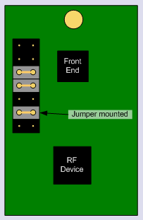
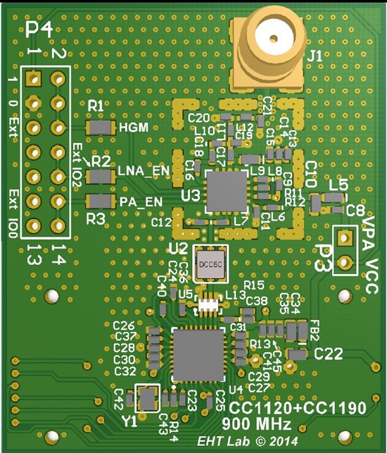
I want to test the CC1120 + CC1190 evaluation module with the SmartRF studio, reading the help software help there is a jumper configuration to be done (P4 pinrow) and GPIOs have to be configured in a certain way for the software to control the CC1190, but from the drawing is not clear to me how to set the jumpers, can you please clarify (from the schematics)?

HGM -> Pin 9 (P1 SMD SOCKET 2x10)

LNA_EN -> Pin 7 (P1 SMD SOCKET 2x10)

PA_EN -> Pin 3 (P1 SMD SOCKET 2x10)

About the GPIO configuration (G0 and G2), what values should I use for IOCFG2 and IOCFG0?

Regards,

--Antonio

  • HGM -> Pin 9 (P1 SMD SOCKET 2x10)

    LNA_EN -> Pin 7 (P1 SMD SOCKET 2x10)

    PA_EN -> Pin 3 (P1 SMD SOCKET 2x10)

    is correct.

    For this setting HGM, LNA_EN and PA_EN are controlled by the MSP430 on the TRXEB so you don't have to set the GPIOs.

  • Sorry for asking again, but this doubt originated when using the SmartRF Studio tool placing the evaluation boards in Packet RX/TX mode and not seeing any activity, but when I replace the CC1120+CC1190 RX end for a plain CC1120 module, I can sniff and receive packets (with 5% PER more or less).  Also in continuous RX/TX mode the LOCK_STATUS is permanently OFF.

    The above jumper settings are meant for this SmartRF Studio tests, or are specific to the built-in TRXEB firmware test? because on the evaluation module quick start guide there is a section describing the setup to work with the SmartRF Studio, and it says to configure the GPIO0/GPIO2 registers when TX/RX.

    Thanks again, sorry for re-posting.

  • - Have you selected CC1190 as frontend in SmartRF Studio?

    - The CC1120+CC1190 board can be controlled two different ways from SmartRF Studio:

    For both methods you should have the following voltages on CC1190:

    RX: HGM=3V, LNA_EN=3V, PA_EN=0V

    TX: HGM=3V, LNA_EN=0V, PA_EN=3V

    - With the jumper settings used as in the picture in the first post CC1190 is controlled by the MSP430 on the TRXEB given that CC1190 is selected as front end. The user does need to set any values for the GPIOs.

    - The HGM jumper moved to the upper most position (VDD) and the two other jumpers moved one position down (GPIO control) the LNA_EN and PA_EN are controlled by GPIO0/GPIO2 and IOCFG has to be changed dependent on if RX or TX is used.

    IOCFG=0x73 sets the pin high, IOCFG=0x33 sets the pin low.

  • Hi TER,

    Did not want to make a new thread for my question.

    While Smart RF Studio supports CC1120+CC1190 module for 868MHz, there are no such modules in real life.

    I would like to build CC1120+CC1190 module for 915 MHz with the same board shape and connectors as you all eval boards are. The question is - would all settings for testing at 868MHz work at 915MHz as well or I will need to change anything? Would changing Carrier frequency to 915 MHz be enough for that?

  • You don't need to change settings between 868 MHz and 915 MHz except for the frequency word. The reference design is different for 868 and 915 due to the difference between ETSI and FCC but only hardware need to be changed between the 2 frequencies.

  • TER,

    Thanks.

    When you are talking about hardware differences you mean only frequency related parts, right? I did not see another changes in hardware.

  • For the CC112x part of CC1120+CC1190 the BOM is the same for 868 MHz and 915 MHz. For the CC1190 part the filtering is different to handle ETSI vs FCC (2. and 3. harmonic limits are different)

  • Hi TER,

    I could find the difference between them in couple of small changes. For 868 MHz module PA_OUT has additional LC circuitry L25+C210, and C24 across the L23.

    And SAW filters are different.

    Is that the difference you are talking about or I use wrong app notes?

    And I have a question about balun part of the schematic.

    We used CC1200 modules from TI for distance testing. Definitely, we could not get 10 km :-) Roughly about a mile (less than that) on the ground. However, we've found that on one distance receiving signal at 868MHz is about 6dB higher, than at 915MHz.. Since the modules, antennas, etc are same, we think this mostly might be a difference in discrete balun frequency response. Because of that I think about using integral baluns for the particular frequency ranges - 866 and 915 MHz. What do you think about that?

    And when I drew schematic for CC1120+CC1190 I originally used discrete balun directly from the AppNote. And after it's been drawn I tried to simulate the balun using spice simulator built in to Altium Designer. I guess, because of it's limitation, I could not get result I expected.  It did not work with symmetrical source, and with asymmetrical provided result with maximum above 1 GHz. There was no any difference between 866 and 915 MHz. Do you have Spice simulation results for the baluns used in Appnotes?

  • The balun for CC1200 is designed to have a close to flat response in the frequency range from 868 MHz and 915 MHz. The sensitivity change with about 0.5 dB between the two frequencies and the output power is 1 dB lower at 915 MHz compared with 868 MHz. The later is due to the frequency response of the PA, not the balun. 

    => The gain is very limited by trying to redimension the balun, particularly if you look at the increased risk.

    When you did the tests, did you test at 868 MHz and 915 MHz boards at the same time (exactly the same test conditions). It could also be that the noise at 868 MHz is different from 915 MHz dependent on which band that is used in the region you are testing in. You could also test on 868.1 or something to see if this make a difference.  

  • The balun for CC1200 is designed to have a close to flat response in the frequency range from 868 MHz and 915 MHz. The sensitivity change with about 0.5 dB between the two frequencies and the output power is 1 dB lower at 915 MHz compared with 868 MHz.


    I see. I expected to have some filtering effect. Anyway, 1dB is not too small value when you want to get maximum distance with minimal power consumption.

    What would you say about the integrated baluns by johansontechnology They have separated for 915 and 866 MHz. They take less space on board than discrete ones. I contacted to them. Their engineer said that the baluns I asked about, were designed specifically for TI chips.

    The later is due to the frequency response of the PA, not the balun.


    The CC1200 eval modules come without PA. However, it might be antenna. We bought recently 5dBi antennas from one company (don't remember now), they have separate 915 and 866 MHz antennas.

    => The gain is very limited by trying to redimension the balun, particularly if you look at the increased risk.

    Please, make this statement more clear.

    When you did the tests, did you test at 868 MHz and 915 MHz boards at the same time (exactly the same test conditions).


    Yes. We used standalone boards and just changed the frequency for the PER testing . Did not believe to the result from the first time and immediately repeated the test by switching the frequency back and force. The result was same. That is why I came to idea of the balun. On this module it is the only frequency dependable circuitry.

  • I don't know, why my previous posting has gray color. Tried to change to black but could not.

  • For the integrated balun: see http://www.ti.com/lit/an/swra407/swra407.pdf You loose a few dB in the link budget using this.

  • Thanks for the appnote.

    Seems like the ideal case for our design would be using discrete design with ML inductors, but using integrated balun still might be acceptable choice.

    Would you inspect my schematic when I finish it?

  • I can take a quick look at the schematic when you are done.

  • Hi TER,

    Please, take a look

    4477.RF_Module.PDF

    It based on CC1120+CC1190 appnote, but balun changed to integral one.

    If you think anything better to be added or taken out, please. let me know.

  • L13 should be 10 nH, other than that I have no comments.

  • I think L5, L6, L8, L13 could have the same inductance - 15 nH. It will make BOM easy. All of them provide power and bigger inductance will make the power cleaner. What do you think?

  • Not a good idea. L13 is part of the impedance the PA sees and the value used in the ref design gives the best performance. The same is the case with L6 and L8, the value have impact on the impedance the LNA/ PA sees and hence the performance.

  • I see, thanks.

    What about the L13, then?

    In the app notes those inductors (L171) are 8n2, but your recommendation is 10nF. Is it later value found after the app notes release? Or that change made because of using integral balun?

  • Which app note are you referring to? In this http://www.ti.com/tool/cc112x-ipc-4l-868rd the value is 10 nH.

  • I started from this: http://www.ti.com/tool/cc1120-cc1190em915rd and similar for 868MHz with discrete baluns. Probably just did not pay attention to the difference in power inductor for these appnotes.

  • When using the IPC this inductor had to be changed to optimize sensitivity.

  • One more question.

    I'm going to use primarily MCL inductors. Are there places where WW (wired) inductors must be used?

  • If possible use it for the CC1190 part. I'm not sure how the output power/ impedances will change if using MCL here.

  • I think to use WW for CC1190 powering and outputs. Low level signals (on the "left side" of the CC1190) should not be affected by using MCL. Besides, the integral balun is MCL anyway :-)

  • Hi TER,

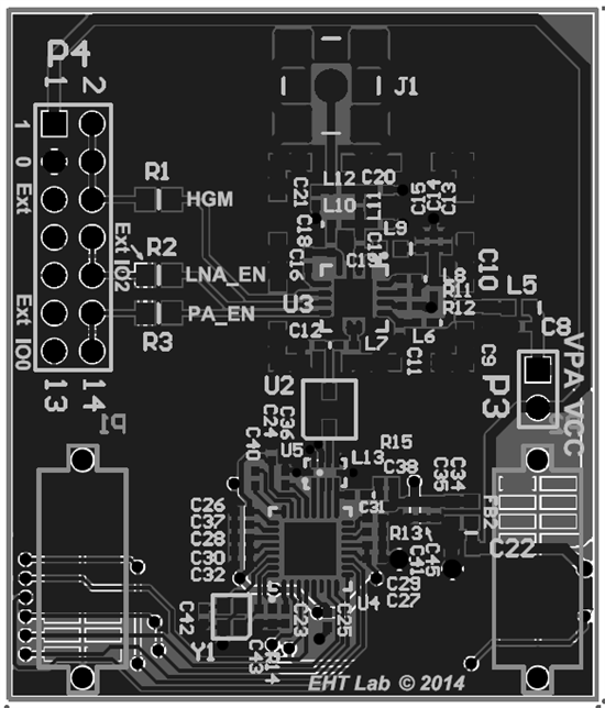
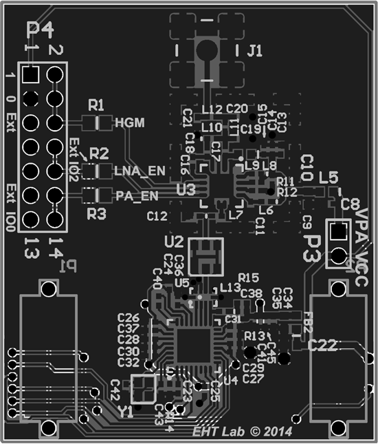
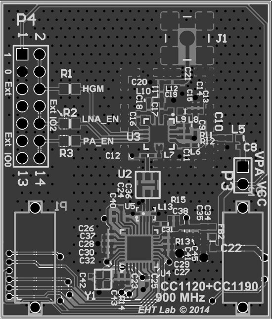
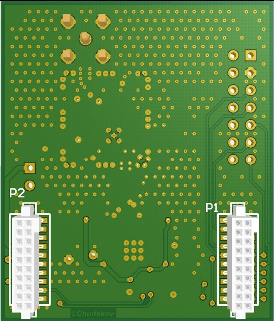
    Here are pictures of my layout: top layer gerber, board drawing and two 3D pictures. Stitches will do later before sending to fab.

    Please, take a look.

  • - Looking at the 3-D plot it looks like not all vias under CC112x and CC1190 are connected to the ground plane on the other side of the board.

    - Check the recommended layout for the SAW filter. (check Epcos website)

  • Fixed the library and made some additional small changes

  • The  first time I looked at this I think I didn't see clearly which caps were where. The placement of C20 and C19 is not optimal. The ground connection for those two are fairly close to each other and part of the signal could go here instead of being filtered. Looking at the layout it should be possible to move the SMA to the right and swap C20 and L12. C20 and C19 should point in opposite direction.

  • TER,

    That is interesting point about moving the SMA to the other whole in the RF shield and changing L&C places accordingly. Will do and post again.

    Thanks.

  • TER,

    Moving the connector to the right side makes the output trace longer. Originally I tried to do it as short as possible. Anyway, please, take a look

  • The track is still short, no problem. It looks like you have forgotten a couple of vias on the ground connection point of C20/ C21?

  • Honestly, I thought that since I already have ground everywhere, I could eliminate those vias. Wrong assumption? Ok, I will put them back when finalize the board. Need stitching anyway.

    What about anything else?

    I also thought about partial separating of digital and analog RF ground that they would connect only in one place in the middle or on side of the board. Do you think it might be useful?

  • Put back the vias.

    Anything else except stitching?

  • Yes, a decoupling cap should always have a via to ground. Looks like you need more vias around the radio. I assume you use the same stack-up as the ref design.

  • TER,

    Ok, I will put vias for the decoupling caps.

    For this board I actually want to use 2 layers, because in the appnote you recommended I discovered that  2 layers design is not much worse than 4 layers. And this board is only for testing whether we can get longer distance than with some other boards we already have on hands. And how much longer.   If yes, the real board will have 4 layers.

    And 2 layers boards are cheaper to fab, too. :-)

    So, if there are any specific  recommendations for 2 layers board before I finalize the design, I'll be glad to get them.

    If it is interesting I will share our measured data in here in comparing to CC1200 and CC1101+CC1190 boards.

  • Normally we recommend a 4 layer design for a combo using CC1190. Mainly two reasons for this:

    - Ground. Most 2 layer boards I have seen has a poorer ground plane compared to 4 layers. In you case the ground looks good as far as I can see

    - The impedance change. With a 2 layer design the ground vias have larger impedance than in a 4 layer design. The impedances in the ref design are tuned with 0.4mm between the signal and the ground layer. If you use a 2 layer board the distance is typically x2 or x3.

    When using +27 dBm the power level is high requiring a good layout. Not sure if a 2 layer design will work.

  • TER,

    Anyway, the fab where I make my prototypes has thicker board than TI eval modules.

    I think, even if I can't get +27dBm I should get power higher than CC1200 module alone with its 14dBm. So, I will take a risk :-)

    Just in case, please take a last (hopefully last) look.

  • Looks good, let us know the performance when you have tested some

  • Unfortunately I have found an error in the layout when the boards came form fab. The connectors were mirrored. So, I had to make some rework and reorder the boards. Hopefully will get them back in the end of the next week. 

  • Hi Igor & TI,

    C8 in your schematic is 0.22uF = 220nF. In the TI schematic this cap is 220pF. Is this intentional?

    TI: Also, I guess the LC (L5 [TI: L2]) filter is put there in order to filter RF noise from the local CC1190 power plane from entering the "outside world". I also see that this inductor is 11nH. This increases the unique BOM count. There is another 10nH used after the SAW filter. Has TI tested the power-filter with a 10 nH for RF leakage? Any reason why it is not used a ferrite bead like on the power filter for cc1120?

    Best Regards,

    HC

  • Hi Hans,

    C8. No, it is not intentional, just misreading from the AppNote. I don't think the capacitor value here is too important, but I'll try to put there something closer to 220pF, may be 1000 pF (C14). Don't want to order just this part and don't have too many 0402 components around. Thanks for this note.

    L5 (TI:L2). I asked TER about this inductor. Wanted to use 15nH (bigger is better :)) or even ferrite bead. However, he recommended to not change this value. You can check in early conversation. Since this is my first RF project in engineering life (the latest was long time ago in university :-)) I decided to follow his recommendation

  • Hi Igor,

    you're welcome :)

    I read through the discussion, and in his reply:

    "Not a good idea. L13 is part of the impedance the PA sees and the value used in the ref design gives the best performance. The same is the case with L6 and L8, the value have impact on the impedance the LNA/ PA sees and hence the performance."

    ... he does not comment on L5 as far as I can see. I think the 220pF and this inductor is intended as a LP filter in order to filter RF noise created at the local RF power plane from leaving this local power plane and entering the "outer world". I guess the cutoff frequency here could be altered a bit without much influence on performance. Even further filtering would improve the leakage if necessary I believe.


    HC

  • TER,

    Here is the very preliminary result. We ran simple TER test with TrxEB boards in standalone mode comparing this module with TI's CC1101+CC1190. I believe the TI module is 4 layers.

    Distance between the "stations" is ~0.15 mile, frequency 915 MHz, all PER = 0%

    CC1101 + CC1190 + 2dBi antenna - -70dB

    CC1101 + CC1190 + 5dBi antenna - -55dB

    CC1120 + CC1190 + 5dBi antenna - -62dB

    My module is 2 layers and does not have RF shield soldered in place. I'm going to solder it tonight and will try to measure the signal level tomorrow again. Stay tuned :-)

    TER, we've got a problem with one TrxEB board. Smart Studio can recognize the modules (all three of them: CC1200, CC1101+CC1190, CC1120+CC1190), but seems like they could not be controlled through USB. When I try to read packets, the Smart Studio neither can read the packet, nor read RSSI. And even  when I try to stop the process, it does not stop. I need to power off the board for that. However, in continues RX reading mode it shows RSSI. If I try to use this board to send packets, the other board does show even RSSI, i.e., I guess, nothing is transmitted from the bad board under PC control.

    In standalone mode both boards work fine.

    What can I do to fix it? Is it fixable at all?

  • Hi Igor,

    off topic: could you give a link to where you have found a 5dBi antenna please?

    Regards, HC

  • Hi HC,

    We use these antennas

    http://www.l-com.com/wireless-antenna-900-mhz-5dbi-rubber-duck-antenna-sma-male-connector

  • Tested my module (CC1120 + CC1190) with RF shield. Got quite interesting results at the same location

    Without shield (previous result) - -62dB

    With RF Shield

    @1.2kbit  - -59dB

    @50kbit - went from ~-73 to -57dB and this level was staying all the way when we were closing without dropping packets. Seems like CC1120 has a quite good internal AGC on RX side.

    When previously we did the same with CC1101+CC1190, the signal level increased and at distance about 5 yards the level reached ~-40dB and packets were lost due signal level overloading.

    ==========================================

    Next steps:

    • Checking the maximum distance in real life: LoS with antennas about 5 feet above ground. Will be processed either end of this week or beginning of the next one.
    • Maybe: 4 layers board with the same schematic. In about 1 month or a little more. My inexpensive shuttle fab makes 4 layers boards in about 4 weeks.

    Stay tuned :-)

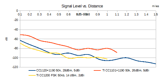
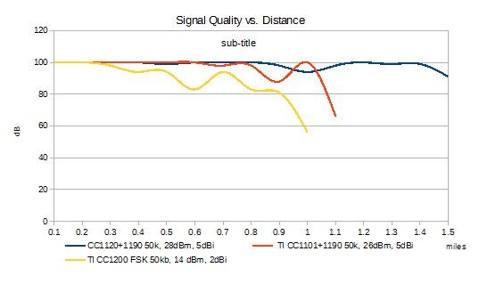
  • Finally made distance testing

    Distance CC1120+1190 50k, 28dBm, 5dBi TI CC1101+1190 50k, 26dBm, 5dBi TI CC1200 FSK 38.4kb, 14 dBm, 2dBi
    miles Level (dB) Quality(%) Level (dB) Quality (%) Level (dB) Quality (%)
    0.1 -63 100 -51 100 -69 100
    0.2 -72 100 -54 100 -79 100
    0.3 -80 100 -63 100 -85 98
    0.4 -89 100 -67 100 -90 94
    0.5 -93 99 -72 100 -91 94
    0.6 -90 100 -77 100 -101 83
    0.7 -95 100 -83 98 -99 94
    0.8 -93 100 -80 98 -100 83
    0.9 -102 98 -83 88 -99 81
    1 -106 94 -80 100 -103 56
    1.1 -103 98 -89 66
    1.2 -100 100
    1.3 -106 99
    1.4 -109 99
    1.5 -113 91

    In graphical  view

    TER, I have a question.

    We found the following behavior (that was noticed early as well with other modules): the modules can keep connection for long distance, but they can link only up to 1.1 miles. What is the difference between keeping link and making the link. I would assume, that if modules can see each other, there should not be a problem to link. Is it not?

  • Not sure what type of software you are running. It sounds like the linking require higher SNR than keeping the link.