This thread has been locked.

If you have a related question, please click the "Ask a related question" button in the top right corner. The newly created question will be automatically linked to this question.

CANBUS communication Receive Problem

Other Parts Discussed in Thread: TMS320F28335, SN65HVD233-HT, ISO1050EVM, ISO1050

Hi Trey,

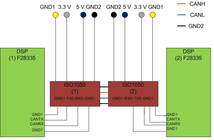
I have faced a trouble with CAN communication.I'm workin on Delfino experimenter kit has F28335 controlCard.

My problem is;
I have 2 nodes on the CAN Bus .One of them is listener,the other one is talker.There is no problem with talker but the listener.I'm trying to realize  the listener node.I changed the code of the ssqc019 lab11_2 according to my desires.I can build the new code but it does not work on the circuit.I have a doubt I miss something on the code.
When I debug the code,code does not entire the condition of
 if(ECanaRegs.CANRMP.bit.RMP1== 1 ) // control valid new data in MBX1?
we can say there is an assigning mistake with ID?
or overwritten problem occurs?
duties of nodes:
Talker node sends 4 byte data every 10 ms with ID=2005 (integer) @ 208.333kbit/s
Listener node receives these data and display on 16 leds  @208.333kbit/s
I added 3 files changed myself.(btw there is no linking problem)
Please let me know what I have missed?(I added neccessary some notes respect to changes)
4118.canreceivernode.txt
//
//      Lab5_1: TMS320F28335
//      (c) Frank Bormann
//
//###########################################################################
//
//
// FILE:	Lab11_2.c
// 
// TITLE:	CAN - Receive via F28335controlCARD 
//			and SH65HVD230 at Peripheral Explorer Board
//
//			Extended CAN-Frame is received with 100 kbit/s
//
//			Objective:  
//			Receive a 1 Byte data frame with Identifier 0x10000000  
//			and display 4 least significant bits of byte0 at  4 LEDs
//
//			Mailbox 1 is receiver
//			Identifier : 0x1000 0000 
//			Data Length Code (DLC) =  1
//			eCANA is at GPIO31 (CANTXA) and GPIO30 (CANRXA)
// 
// 			Frequency Osscillator @F28335controlCARD: 30MHz
// 			PLLCR = 10   :  multiply by 5  
// 			SYSCLKOUT = 150MHz , 28335-CAN-CLKIN = 75MHz
//			CAN - Bit timing set in file "DSP2833x_ECan.c" for 100 kbit/s:
//		    TQ = (49 +1) / 75 MHz = 0.667 us:   BRPREG = 49
//		    tseg1 = 1us (10+1)     = 7.333 us; 	TSEG1REG = 10
//			tseg2 = 1us (2+1)	  = 2 us;	TSEG2REG = 2
//   By A.A
//Editing:    Used F28335 controlCARD Release 2.2,TMDSCNCD28335 R2.2
//               Extended Can frame is received with 208.33 kbit/s
//               objective:
//                     Receive 4 byte data frame with identifier 0x000007D5 // unsigned long ID= 2005               
//                     eCANA is at GPIO31 (CANTXA) and GPIO30 (CANRXA)
//                     Frequency Osscillator @F28335controlCARD: 30MHz
// 			PLLCR = 10   :  multiply by 5  
// 			SYSCLKOUT = 150MHz , 28335-CAN-CLKIN = 75MHz
//			CAN - Bit timing set in file "DSP2833x_ECan.c" for 208.33 kbit/s:
//		    TQ = (23 +1) / 75 MHz = 0.32 us:   BRPREG = 23
//		    tseg1 = 0.32u*(10+1)     = 3.52 us; 	TSEG1REG = 10
//			tseg2 = 0.32u* (2+1)	  = 0.96 us;	TSEG2REG = 2
//                    tcan=tseg1+tseg2+TQ=3.52+0.96+0.32=4,8u => 208,3333333kbit/s   
//    
//          GPIO pins are used to display the received data on 16 leds 
//    This written code for listener  node whose talker node sends 4 byte data every 10ms
// 
//###########################################################################
//  Ver | dd mmm yyyy | Who  | Description of changes
// =====|=============|======|===============================================
//  3.0 | 02 May 2008 | F.B. | Lab5_1 for F28335; 
//  3.1 | 06 Nov 2009 | F.B  | Lab5_1 for F28335 and PE revision5
//###########################################################################
#include "DSP2833x_Device.h"

// external function prototypes
extern void InitSysCtrl(void);
extern void InitPieCtrl(void);
extern void InitPieVectTable(void);
extern void InitCpuTimers(void);
extern void InitECan(void);
extern void ConfigCpuTimer(struct CPUTIMER_VARS *, float, float);
extern void InitECan(void);
// Prototype statements for functions found within this file.
void Gpio_select(void);//I/O se�imi,register ayarlar1
interrupt void cpu_timer0_isr(void);


//###########################################################################
//						main code									
//###########################################################################
void main(void)
{
	
   struct	ECAN_REGS ECanaShadow;		// local copy of CANA registers
  
  Uint16 temp;//1st byte
  Uint16 temp2;//2nd byte
  Uint16 temp3;//3th byte
  Uint16 temp4;//4th byte
  
  InitSysCtrl();	// Basic Core Init from DSP2833x_SysCtrl.c
  
    EALLOW;
   	SysCtrlRegs.WDCR= 0x00AF;	// Re-enable the watchdog 
   	EDIS;			// 0x00AF  to NOT disable the Watchdog, Prescaler = 64

	DINT;				// Disable all interrupts
	
	Gpio_select();		
    
   /* Initialize the CAN module */
	// NOTE: first modify TI-file: InitECan() to 100kbps by setting BTR = 49
        //edit:changed the values to 208.33kbps by setting BTR=23
	InitECan();	
	
	/* Write to Mailbox 1 message ID field		*/
	ECanaMboxes.MBOX1.MSGID.all     = 0x000007D5;	// messsage ID=2005 is set as integer 
    ECanaMboxes.MBOX1.MSGID.bit.IDE = 1;  // Extended Identifier

	
      /* Configure Mailbox 1 as Receiver mailbox */
	ECanaShadow.CANMD.all = ECanaRegs.CANMD.all;	
	ECanaShadow.CANMD.bit.MD1 = 1;
	ECanaRegs.CANMD.all = ECanaShadow.CANMD.all; 
   
   /* Enable Mailbox 1  						*/
	ECanaShadow.CANME.all = ECanaRegs.CANME.all;	
	ECanaShadow.CANME.bit.ME1 = 1;
	ECanaRegs.CANME.all = ECanaShadow.CANME.all; 


    InitPieCtrl();		// clear all pending PIE-Interrupts and to disable all PIE interrupt lines
	
	InitPieVectTable();	// default ISR's in PIE,This function will initialize the PIE-memory to an initial state.
	
	EALLOW;//Cputimeri PIE icerisinden re-map ediyoruz
	PieVectTable.TINT0 = &cpu_timer0_isr;
	EDIS;
	
	InitCpuTimers();	// basic setup CPU Timer0, 1 and 2,Timer0 set edildi

	ConfigCpuTimer(&CpuTimer0,150,100000); // CPU - Timer0 at 100 milliseconds
	//parametre1=adress of core,parametre2=internal speed of DSP,paramtre3=period time for timer overflow
	

	PieCtrlRegs.PIEIER1.bit.INTx7 = 1;//to enable interupt mask of cputimer

	IER |=1;//enable interrupt core INT1

	EINT;//enable control interrupt lines 2 macros
	ERTM;//.......

	CpuTimer0Regs.TCR.bit.TSS = 0;	// start timer0
	
	
	while(1)
	{    
	  		while(CpuTimer0.InterruptCount == 0);
			CpuTimer0.InterruptCount = 0;
			
			EALLOW;
			SysCtrlRegs.WDKEY = 0x55;	// service WD #1
			EDIS;
			
			 if(ECanaRegs.CANRMP.bit.RMP1== 1 ) // control valid new data in MBX1?
			{
			 	temp = ECanaMboxes.MBOX1.MDL.byte.BYTE0;	// byte zero read message,load it temp,		
				temp2=ECanaMboxes.MBOX1.MDL.byte.BYTE1;
				temp3=ECanaMboxes.MBOX1.MDL.byte.BYTE2;
				temp4=ECanaMboxes.MBOX1.MDL.byte.BYTE3;
				ECanaRegs.CANRMP.bit.RMP1 = 1;	// clear the status flag RMP1          
	
	if(temp&1) GpioDataRegs.GPBSET.bit.GPIO59=1;
	           else GpioDataRegs.GPBCLEAR.bit.GPIO59 = 1;
	if(temp&2) GpioDataRegs.GPBSET.bit.GPIO61=1; 
	            else GpioDataRegs.GPBCLEAR.bit.GPIO61=1;
	 if(temp&4) GpioDataRegs.GPASET.bit.GPIO1=1;
	            else GpioDataRegs.GPACLEAR.bit.GPIO1=1;
	 if(temp&8) GpioDataRegs.GPASET.bit.GPIO3=1;
	            else GpioDataRegs.GPACLEAR.bit.GPIO3=1;  
	 if(temp2&1) GpioDataRegs.GPASET.bit.GPIO5=1;
	            else GpioDataRegs.GPACLEAR.bit.GPIO5=1;                                              	
	if(temp2&2) GpioDataRegs.GPASET.bit.GPIO7=1;
	            else GpioDataRegs.GPACLEAR.bit.GPIO7=1;
	if(temp2&4) GpioDataRegs.GPASET.bit.GPIO9=1;
	            else GpioDataRegs.GPACLEAR.bit.GPIO9=1;              		
	if(temp2&8) GpioDataRegs.GPASET.bit.GPIO11=1; 
                 else GpioDataRegs.GPACLEAR.bit.GPIO11=1; 				
     if(temp3&1) GpioDataRegs.GPBSET.bit.GPIO49=1;
	            else GpioDataRegs.GPBCLEAR.bit.GPIO49=1;              		
	if(temp3&2) GpioDataRegs.GPCSET.bit.GPIO85=1; 
	            else GpioDataRegs.GPCCLEAR.bit.GPIO85=1; 
	if(temp3&4) GpioDataRegs.GPASET.bit.GPIO13=1; 
	            else GpioDataRegs.GPACLEAR.bit.GPIO13=1; 
	if(temp3&8) GpioDataRegs.GPASET.bit.GPIO14=1; 
	            else GpioDataRegs.GPACLEAR.bit.GPIO14=1; 
	if(temp4&1) GpioDataRegs.GPASET.bit.GPIO25=1; 
	            else GpioDataRegs.GPACLEAR.bit.GPIO25=1; 
	if(temp4&2) GpioDataRegs.GPASET.bit.GPIO21=1;
	            else GpioDataRegs.GPACLEAR.bit.GPIO21=1;
	 if(temp4&4) GpioDataRegs.GPASET.bit.GPIO23=1; 
	            else GpioDataRegs.GPACLEAR.bit.GPIO23=1;
    if(temp4&8) GpioDataRegs.GPASET.bit.GPIO29=1;
	            else GpioDataRegs.GPACLEAR.bit.GPIO29=1;   			
			}
	}
} 

void Gpio_select(void)
{
	EALLOW;
	GpioCtrlRegs.GPAMUX1.all = 0;	// GPIO15 ... GPIO0 = General Puropse I/O
	GpioCtrlRegs.GPAMUX2.all = 0;	// GPIO31 ... GPIO16 = General Purpose I/O
	
	GpioCtrlRegs.GPAMUX2.bit.GPIO30 = 1;	// CANA_RX
	GpioCtrlRegs.GPAMUX2.bit.GPIO31 = 1;	// CANA_TX
	
	GpioCtrlRegs.GPBMUX1.all = 0;	// GPIO47 ... GPIO32 = General Purpose I/O
	GpioCtrlRegs.GPBMUX2.all = 0;	// GPIO63 ... GPIO48 = General Purpose I/O
	
	GpioCtrlRegs.GPCMUX1.all = 0;	// GPIO79 ... GPIO64 = General Purpose I/O
	GpioCtrlRegs.GPCMUX2.all = 0;	// GPIO87 ... GPIO80 = General Purpose I/O
	 
	GpioCtrlRegs.GPADIR.all = 0;
	GpioCtrlRegs.GPADIR.bit.GPIO1=1;
	GpioCtrlRegs.GPADIR.bit.GPIO3=1;
	GpioCtrlRegs.GPADIR.bit.GPIO5=1;
	GpioCtrlRegs.GPADIR.bit.GPIO7=1;
	GpioCtrlRegs.GPADIR.bit.GPIO9=1;
	GpioCtrlRegs.GPADIR.bit.GPIO11=1;
	GpioCtrlRegs.GPADIR.bit.GPIO13=1;
	GpioCtrlRegs.GPADIR.bit.GPIO14=1;
	GpioCtrlRegs.GPADIR.bit.GPIO25=1;
	GpioCtrlRegs.GPADIR.bit.GPIO27=1;
	GpioCtrlRegs.GPADIR.bit.GPIO21=1;
	GpioCtrlRegs.GPADIR.bit.GPIO23=1;
	GpioCtrlRegs.GPADIR.bit.GPIO29=1;
	
	
	GpioCtrlRegs.GPBDIR.all = 0;     // GPIO63-32 as inputs
	GpioCtrlRegs.GPBDIR.bit.GPIO49=1;
	GpioCtrlRegs.GPBDIR.bit.GPIO59=1;
	GpioCtrlRegs.GPBDIR.bit.GPIO61=1;
	
    GpioCtrlRegs.GPCDIR.all=0;//lines in c will be digital input
	GpioCtrlRegs.GPCDIR.bit.GPIO85=1;
	
	EDIS;
}   
interrupt void cpu_timer0_isr(void)
{
	CpuTimer0.InterruptCount++;
	EALLOW;
	SysCtrlRegs.WDKEY = 0xAA;	// service WD #2
	EDIS;
	PieCtrlRegs.PIEACK.all = PIEACK_GROUP1;
}
//===========================================================================
// End of SourceCode.
//===========================================================================
7711.DSP2833x_ECan.txt
// TI File $Revision: /main/8 $
// Checkin $Date: June 25, 2008   15:19:07 $
//###########################################################################
//
// FILE:	DSP2833x_ECan.c
//
// TITLE:	DSP2833x Enhanced CAN Initialization & Support Functions.
//
//###########################################################################
// $TI Release: DSP2833x/DSP2823x C/C++ Header Files V1.31 $
// $Release Date: August 4, 2009 $
//###########################################################################

#include "DSP2833x_Device.h"     // DSP2833x Headerfile Include File
#include "DSP2833x_Examples.h"   // DSP2833x Examples Include File


//---------------------------------------------------------------------------
// InitECan:
//---------------------------------------------------------------------------
// This function initializes the eCAN module to a known state.
//
void InitECan(void)
{
   InitECana();
#if DSP28_ECANB
   InitECanb();
#endif // if DSP28_ECANB
}

void InitECana(void)		// Initialize eCAN-A module
{
/* Create a shadow register structure for the CAN control registers. This is
 needed, since only 32-bit access is allowed to these registers. 16-bit access
 to these registers could potentially corrupt the register contents or return
 false data. This is especially true while writing to/reading from a bit
 (or group of bits) among bits 16 - 31 */

struct ECAN_REGS ECanaShadow;

	EALLOW;		// EALLOW enables access to protected bits

/* Configure eCAN RX and TX pins for CAN operation using eCAN regs*/

    ECanaShadow.CANTIOC.all = ECanaRegs.CANTIOC.all;
    ECanaShadow.CANTIOC.bit.TXFUNC = 1;
    ECanaRegs.CANTIOC.all = ECanaShadow.CANTIOC.all;

    ECanaShadow.CANRIOC.all = ECanaRegs.CANRIOC.all;
    ECanaShadow.CANRIOC.bit.RXFUNC = 1;
    ECanaRegs.CANRIOC.all = ECanaShadow.CANRIOC.all;

/* Configure eCAN for HECC mode - (reqd to access mailboxes 16 thru 31) */
									// HECC mode also enables time-stamping feature

	ECanaShadow.CANMC.all = ECanaRegs.CANMC.all;
	ECanaShadow.CANMC.bit.SCB = 1;
	ECanaRegs.CANMC.all = ECanaShadow.CANMC.all;

/* Initialize all bits of 'Master Control Field' to zero */
// Some bits of MSGCTRL register come up in an unknown state. For proper operation,
// all bits (including reserved bits) of MSGCTRL must be initialized to zero

    ECanaMboxes.MBOX0.MSGCTRL.all = 0x00000000;
    ECanaMboxes.MBOX1.MSGCTRL.all = 0x00000000;
    ECanaMboxes.MBOX2.MSGCTRL.all = 0x00000000;
    ECanaMboxes.MBOX3.MSGCTRL.all = 0x00000000;
    ECanaMboxes.MBOX4.MSGCTRL.all = 0x00000000;
    ECanaMboxes.MBOX5.MSGCTRL.all = 0x00000000;
    ECanaMboxes.MBOX6.MSGCTRL.all = 0x00000000;
    ECanaMboxes.MBOX7.MSGCTRL.all = 0x00000000;
    ECanaMboxes.MBOX8.MSGCTRL.all = 0x00000000;
    ECanaMboxes.MBOX9.MSGCTRL.all = 0x00000000;
    ECanaMboxes.MBOX10.MSGCTRL.all = 0x00000000;
    ECanaMboxes.MBOX11.MSGCTRL.all = 0x00000000;
    ECanaMboxes.MBOX12.MSGCTRL.all = 0x00000000;
    ECanaMboxes.MBOX13.MSGCTRL.all = 0x00000000;
    ECanaMboxes.MBOX14.MSGCTRL.all = 0x00000000;
    ECanaMboxes.MBOX15.MSGCTRL.all = 0x00000000;
    ECanaMboxes.MBOX16.MSGCTRL.all = 0x00000000;
    ECanaMboxes.MBOX17.MSGCTRL.all = 0x00000000;
    ECanaMboxes.MBOX18.MSGCTRL.all = 0x00000000;
    ECanaMboxes.MBOX19.MSGCTRL.all = 0x00000000;
    ECanaMboxes.MBOX20.MSGCTRL.all = 0x00000000;
    ECanaMboxes.MBOX21.MSGCTRL.all = 0x00000000;
    ECanaMboxes.MBOX22.MSGCTRL.all = 0x00000000;
    ECanaMboxes.MBOX23.MSGCTRL.all = 0x00000000;
    ECanaMboxes.MBOX24.MSGCTRL.all = 0x00000000;
    ECanaMboxes.MBOX25.MSGCTRL.all = 0x00000000;
    ECanaMboxes.MBOX26.MSGCTRL.all = 0x00000000;
    ECanaMboxes.MBOX27.MSGCTRL.all = 0x00000000;
    ECanaMboxes.MBOX28.MSGCTRL.all = 0x00000000;
    ECanaMboxes.MBOX29.MSGCTRL.all = 0x00000000;
    ECanaMboxes.MBOX30.MSGCTRL.all = 0x00000000;
    ECanaMboxes.MBOX31.MSGCTRL.all = 0x00000000;

// TAn, RMPn, GIFn bits are all zero upon reset and are cleared again
//	as a matter of precaution.

	ECanaRegs.CANTA.all	= 0xFFFFFFFF;	/* Clear all TAn bits */

	ECanaRegs.CANRMP.all = 0xFFFFFFFF;	/* Clear all RMPn bits */

	ECanaRegs.CANGIF0.all = 0xFFFFFFFF;	/* Clear all interrupt flag bits */
	ECanaRegs.CANGIF1.all = 0xFFFFFFFF;


/* Configure bit timing parameters for eCANA*/
	ECanaShadow.CANMC.all = ECanaRegs.CANMC.all;
	ECanaShadow.CANMC.bit.CCR = 1 ;            // Set CCR = 1
    ECanaRegs.CANMC.all = ECanaShadow.CANMC.all;

    ECanaShadow.CANES.all = ECanaRegs.CANES.all;

    do
	{
	    ECanaShadow.CANES.all = ECanaRegs.CANES.all;
    } while(ECanaShadow.CANES.bit.CCE != 1 );  		// Wait for CCE bit to be set..

    ECanaShadow.CANBTC.all = 0;

    #if (CPU_FRQ_150MHZ)                       // CPU_FRQ_150MHz is defined in DSP2833x_Examples.h
		/* The following block for all 150 MHz SYSCLKOUT (75 MHz CAN clock) - default. Bit rate = 208.33 khz bps
		   See Note at End of File */
		   //208.33kbit e g�re ayarland�
			ECanaShadow.CANBTC.bit.BRPREG = 23;
			ECanaShadow.CANBTC.bit.TSEG2REG = 2;
			ECanaShadow.CANBTC.bit.TSEG1REG = 10;
    #endif
	#if (CPU_FRQ_100MHZ)                       // CPU_FRQ_100MHz is defined in DSP2833x_Examples.h
	/* The following block is only for 100 MHz SYSCLKOUT (50 MHz CAN clock). Bit rate = 1 Mbps
	   See Note at End of File */
	    ECanaShadow.CANBTC.bit.BRPREG = 4;
		ECanaShadow.CANBTC.bit.TSEG2REG = 1;
		ECanaShadow.CANBTC.bit.TSEG1REG = 6;
	#endif


    ECanaShadow.CANBTC.bit.SAM = 1;
    ECanaRegs.CANBTC.all = ECanaShadow.CANBTC.all;

    ECanaShadow.CANMC.all = ECanaRegs.CANMC.all;
	ECanaShadow.CANMC.bit.CCR = 0 ;            // Set CCR = 0
    ECanaRegs.CANMC.all = ECanaShadow.CANMC.all;

    ECanaShadow.CANES.all = ECanaRegs.CANES.all;

    do
    {
       ECanaShadow.CANES.all = ECanaRegs.CANES.all;
    } while(ECanaShadow.CANES.bit.CCE != 0 ); 		// Wait for CCE bit to be  cleared..

/* Disable all Mailboxes  */
 	ECanaRegs.CANME.all = 0;		// Required before writing the MSGIDs

    EDIS;
}


#if (DSP28_ECANB)
void InitECanb(void)		// Initialize eCAN-B module
{
/* Create a shadow register structure for the CAN control registers. This is
 needed, since only 32-bit access is allowed to these registers. 16-bit access
 to these registers could potentially corrupt the register contents or return
 false data. This is especially true while writing to/reading from a bit
 (or group of bits) among bits 16 - 31 */

struct ECAN_REGS ECanbShadow;

   EALLOW;		// EALLOW enables access to protected bits

/* Configure eCAN RX and TX pins for CAN operation using eCAN regs*/

    ECanbShadow.CANTIOC.all = ECanbRegs.CANTIOC.all;
    ECanbShadow.CANTIOC.bit.TXFUNC = 1;
    ECanbRegs.CANTIOC.all = ECanbShadow.CANTIOC.all;

    ECanbShadow.CANRIOC.all = ECanbRegs.CANRIOC.all;
    ECanbShadow.CANRIOC.bit.RXFUNC = 1;
    ECanbRegs.CANRIOC.all = ECanbShadow.CANRIOC.all;

/* Configure eCAN for HECC mode - (reqd to access mailboxes 16 thru 31) */

	ECanbShadow.CANMC.all = ECanbRegs.CANMC.all;
	ECanbShadow.CANMC.bit.SCB = 1;
	ECanbRegs.CANMC.all = ECanbShadow.CANMC.all;

/* Initialize all bits of 'Master Control Field' to zero */
// Some bits of MSGCTRL register come up in an unknown state. For proper operation,
// all bits (including reserved bits) of MSGCTRL must be initialized to zero

    ECanbMboxes.MBOX0.MSGCTRL.all = 0x00000000;
    ECanbMboxes.MBOX1.MSGCTRL.all = 0x00000000;
    ECanbMboxes.MBOX2.MSGCTRL.all = 0x00000000;
    ECanbMboxes.MBOX3.MSGCTRL.all = 0x00000000;
    ECanbMboxes.MBOX4.MSGCTRL.all = 0x00000000;
    ECanbMboxes.MBOX5.MSGCTRL.all = 0x00000000;
    ECanbMboxes.MBOX6.MSGCTRL.all = 0x00000000;
    ECanbMboxes.MBOX7.MSGCTRL.all = 0x00000000;
    ECanbMboxes.MBOX8.MSGCTRL.all = 0x00000000;
    ECanbMboxes.MBOX9.MSGCTRL.all = 0x00000000;
    ECanbMboxes.MBOX10.MSGCTRL.all = 0x00000000;
    ECanbMboxes.MBOX11.MSGCTRL.all = 0x00000000;
    ECanbMboxes.MBOX12.MSGCTRL.all = 0x00000000;
    ECanbMboxes.MBOX13.MSGCTRL.all = 0x00000000;
    ECanbMboxes.MBOX14.MSGCTRL.all = 0x00000000;
    ECanbMboxes.MBOX15.MSGCTRL.all = 0x00000000;
    ECanbMboxes.MBOX16.MSGCTRL.all = 0x00000000;
    ECanbMboxes.MBOX17.MSGCTRL.all = 0x00000000;
    ECanbMboxes.MBOX18.MSGCTRL.all = 0x00000000;
    ECanbMboxes.MBOX19.MSGCTRL.all = 0x00000000;
    ECanbMboxes.MBOX20.MSGCTRL.all = 0x00000000;
    ECanbMboxes.MBOX21.MSGCTRL.all = 0x00000000;
    ECanbMboxes.MBOX22.MSGCTRL.all = 0x00000000;
    ECanbMboxes.MBOX23.MSGCTRL.all = 0x00000000;
    ECanbMboxes.MBOX24.MSGCTRL.all = 0x00000000;
    ECanbMboxes.MBOX25.MSGCTRL.all = 0x00000000;
    ECanbMboxes.MBOX26.MSGCTRL.all = 0x00000000;
    ECanbMboxes.MBOX27.MSGCTRL.all = 0x00000000;
    ECanbMboxes.MBOX28.MSGCTRL.all = 0x00000000;
    ECanbMboxes.MBOX29.MSGCTRL.all = 0x00000000;
    ECanbMboxes.MBOX30.MSGCTRL.all = 0x00000000;
    ECanbMboxes.MBOX31.MSGCTRL.all = 0x00000000;

// TAn, RMPn, GIFn bits are all zero upon reset and are cleared again
//	as a matter of precaution.

	ECanbRegs.CANTA.all	= 0xFFFFFFFF;	/* Clear all TAn bits */

	ECanbRegs.CANRMP.all = 0xFFFFFFFF;	/* Clear all RMPn bits */

	ECanbRegs.CANGIF0.all = 0xFFFFFFFF;	/* Clear all interrupt flag bits */
	ECanbRegs.CANGIF1.all = 0xFFFFFFFF;


/* Configure bit timing parameters for eCANB*/

	ECanbShadow.CANMC.all = ECanbRegs.CANMC.all;
	ECanbShadow.CANMC.bit.CCR = 1 ;            // Set CCR = 1
    ECanbRegs.CANMC.all = ECanbShadow.CANMC.all;

    ECanbShadow.CANES.all = ECanbRegs.CANES.all;

    do
	{
	    ECanbShadow.CANES.all = ECanbRegs.CANES.all;
	} while(ECanbShadow.CANES.bit.CCE != 1 ); 		// Wait for CCE bit to be  cleared..


    ECanbShadow.CANBTC.all = 0;

    #if (CPU_FRQ_150MHZ)                       // CPU_FRQ_150MHz is defined in DSP2833x_Examples.h
	/* The following block for all 150 MHz SYSCLKOUT (75 MHz CAN clock) - default. Bit rate = 1 Mbps
	   See Note at end of file */
		ECanbShadow.CANBTC.bit.BRPREG = 4;
		ECanbShadow.CANBTC.bit.TSEG2REG = 2;
		ECanbShadow.CANBTC.bit.TSEG1REG = 10;
	#endif
	#if (CPU_FRQ_100MHZ)                       // CPU_FRQ_100MHz is defined in DSP2833x_Examples.h
	/* The following block is only for 100 MHz SYSCLKOUT (50 MHz CAN clock). Bit rate = 1 Mbps
	   See Note at end of file */
	    ECanbShadow.CANBTC.bit.BRPREG = 4;
		ECanbShadow.CANBTC.bit.TSEG2REG = 1;
		ECanbShadow.CANBTC.bit.TSEG1REG = 6;
	#endif

    ECanbShadow.CANBTC.bit.SAM = 1;
    ECanbRegs.CANBTC.all = ECanbShadow.CANBTC.all;

    ECanbShadow.CANMC.all = ECanbRegs.CANMC.all;
	ECanbShadow.CANMC.bit.CCR = 0 ;            // Set CCR = 0
    ECanbRegs.CANMC.all = ECanbShadow.CANMC.all;

    ECanbShadow.CANES.all = ECanbRegs.CANES.all;

    do
    {
        ECanbShadow.CANES.all = ECanbRegs.CANES.all;
    } while(ECanbShadow.CANES.bit.CCE != 0 ); 		// Wait for CCE bit to be  cleared..


/* Disable all Mailboxes  */
 	ECanbRegs.CANME.all = 0;		// Required before writing the MSGIDs

    EDIS;
}
#endif // if DSP28_ECANB


//---------------------------------------------------------------------------
// Example: InitECanGpio:
//---------------------------------------------------------------------------
// This function initializes GPIO pins to function as eCAN pins
//
// Each GPIO pin can be configured as a GPIO pin or up to 3 different
// peripheral functional pins. By default all pins come up as GPIO
// inputs after reset.
//
// Caution:
// Only one GPIO pin should be enabled for CANTXA/B operation.
// Only one GPIO pin shoudl be enabled for CANRXA/B operation.
// Comment out other unwanted lines.


void InitECanGpio(void)
{
   InitECanaGpio();
#if (DSP28_ECANB)
   InitECanbGpio();
#endif // if DSP28_ECANB
}

void InitECanaGpio(void)
{
   EALLOW;

/* Enable internal pull-up for the selected CAN pins */
// Pull-ups can be enabled or disabled by the user.
// This will enable the pullups for the specified pins.
// Comment out other unwanted lines.

	GpioCtrlRegs.GPAPUD.bit.GPIO30 = 0;	    // Enable pull-up for GPIO30 (CANRXA)
//	GpioCtrlRegs.GPAPUD.bit.GPIO18 = 0;	    // Enable pull-up for GPIO18 (CANRXA)

	GpioCtrlRegs.GPAPUD.bit.GPIO31 = 0;	    // Enable pull-up for GPIO31 (CANTXA)
//	GpioCtrlRegs.GPAPUD.bit.GPIO19 = 0;	    // Enable pull-up for GPIO19 (CANTXA)

/* Set qualification for selected CAN pins to asynch only */
// Inputs are synchronized to SYSCLKOUT by default.
// This will select asynch (no qualification) for the selected pins.

    GpioCtrlRegs.GPAQSEL2.bit.GPIO30 = 3;   // Asynch qual for GPIO30 (CANRXA)
//  GpioCtrlRegs.GPAQSEL2.bit.GPIO18 = 3;   // Asynch qual for GPIO18 (CANRXA)


/* Configure eCAN-A pins using GPIO regs*/
// This specifies which of the possible GPIO pins will be eCAN functional pins.

	GpioCtrlRegs.GPAMUX2.bit.GPIO30 = 1;	// Configure GPIO30 for CANRXA operation
//  GpioCtrlRegs.GPAMUX2.bit.GPIO18 = 3;	// Configure GPIO18 for CANRXA operation
	GpioCtrlRegs.GPAMUX2.bit.GPIO31 = 1;	// Configure GPIO31 for CANTXA operation
//  GpioCtrlRegs.GPAMUX2.bit.GPIO19 = 3;	// Configure GPIO19 for CANTXA operation

    EDIS;
}

#if (DSP28_ECANB)
void InitECanbGpio(void)
{
   EALLOW;

/* Enable internal pull-up for the selected CAN pins */
// Pull-ups can be enabled or disabled by the user.
// This will enable the pullups for the specified pins.
// Comment out other unwanted lines.

	GpioCtrlRegs.GPAPUD.bit.GPIO8 = 0;	  // Enable pull-up for GPIO8  (CANTXB)
//  GpioCtrlRegs.GPAPUD.bit.GPIO12 = 0;   // Enable pull-up for GPIO12 (CANTXB)
//  GpioCtrlRegs.GPAPUD.bit.GPIO16 = 0;   // Enable pull-up for GPIO16 (CANTXB)
//  GpioCtrlRegs.GPAPUD.bit.GPIO20 = 0;   // Enable pull-up for GPIO20 (CANTXB)

	GpioCtrlRegs.GPAPUD.bit.GPIO10 = 0;	  // Enable pull-up for GPIO10 (CANRXB)
//  GpioCtrlRegs.GPAPUD.bit.GPIO13 = 0;   // Enable pull-up for GPIO13 (CANRXB)
//  GpioCtrlRegs.GPAPUD.bit.GPIO17 = 0;   // Enable pull-up for GPIO17 (CANRXB)
//  GpioCtrlRegs.GPAPUD.bit.GPIO21 = 0;   // Enable pull-up for GPIO21 (CANRXB)

/* Set qualification for selected CAN pins to asynch only */
// Inputs are synchronized to SYSCLKOUT by default.
// This will select asynch (no qualification) for the selected pins.
// Comment out other unwanted lines.

    GpioCtrlRegs.GPAQSEL1.bit.GPIO10 = 3; // Asynch qual for GPIO10 (CANRXB)
//  GpioCtrlRegs.GPAQSEL1.bit.GPIO13 = 3; // Asynch qual for GPIO13 (CANRXB)
//  GpioCtrlRegs.GPAQSEL2.bit.GPIO17 = 3; // Asynch qual for GPIO17 (CANRXB)
//  GpioCtrlRegs.GPAQSEL2.bit.GPIO21 = 3; // Asynch qual for GPIO21 (CANRXB)

/* Configure eCAN-B pins using GPIO regs*/
// This specifies which of the possible GPIO pins will be eCAN functional pins.

	GpioCtrlRegs.GPAMUX1.bit.GPIO8 = 2;   // Configure GPIO8 for CANTXB operation
//  GpioCtrlRegs.GPAMUX1.bit.GPIO12 = 2;  // Configure GPIO12 for CANTXB operation
//  GpioCtrlRegs.GPAMUX2.bit.GPIO16 = 2;  // Configure GPIO16 for CANTXB operation
//  GpioCtrlRegs.GPAMUX2.bit.GPIO20 = 3;  // Configure GPIO20 for CANTXB operation

	GpioCtrlRegs.GPAMUX1.bit.GPIO10 = 2;  // Configure GPIO10 for CANRXB operation
//  GpioCtrlRegs.GPAMUX1.bit.GPIO13 = 2;  // Configure GPIO13 for CANRXB operation
//  GpioCtrlRegs.GPAMUX2.bit.GPIO17 = 2;  // Configure GPIO17 for CANRXB operation
//  GpioCtrlRegs.GPAMUX2.bit.GPIO21 = 3;  // Configure GPIO21 for CANRXB operation

    EDIS;
}
#endif // if DSP28_ECANB

/*
Note: Bit timing parameters must be chosen based on the network parameters such
as the sampling point desired and the propagation delay of the network.
The propagation delay is a function of length of the cable, delay introduced by
the transceivers and opto/galvanic-isolators (if any).

The parameters used in this file must be changed taking into account the above
mentioned factors in order to arrive at the bit-timing parameters suitable
for a network.

*/
7701.DSP2833x_Examples.txt
// TI File $Revision: /main/9 $
// Checkin $Date: July 2, 2008   14:31:12 $
//###########################################################################
//
// FILE:   DSP2833x_Examples.h
//
// TITLE:  DSP2833x Device Definitions.
//
//###########################################################################
// $TI Release: DSP2833x/DSP2823x C/C++ Header Files V1.31 $
// $Release Date: August 4, 2009 $
//###########################################################################

#ifndef DSP2833x_EXAMPLES_H
#define DSP2833x_EXAMPLES_H


#ifdef __cplusplus
extern "C" {
#endif


/*-----------------------------------------------------------------------------
      Specify the PLL control register (PLLCR) and divide select (DIVSEL) value.
-----------------------------------------------------------------------------*/
//#define DSP28_DIVSEL   0   // Enable /4 for SYSCLKOUT
//#define DSP28_DIVSEL   1 // Enable /4 for SYSCKOUT
#define DSP28_DIVSEL     2 // Enable /2 for SYSCLKOUT
//#define DSP28_DIVSEL     3 // Enable /1 for SYSCLKOUT

#define DSP28_PLLCR   10
//#define DSP28_PLLCR    9
//#define DSP28_PLLCR    8
//#define DSP28_PLLCR    7
//#define DSP28_PLLCR    6
//#define DSP28_PLLCR    5
//#define DSP28_PLLCR    4
//#define DSP28_PLLCR    3
//#define DSP28_PLLCR    2
//#define DSP28_PLLCR    1
//#define DSP28_PLLCR    0  // PLL is bypassed in this mode
//----------------------------------------------------------------------------


/*-----------------------------------------------------------------------------
      Specify the clock rate of the CPU (SYSCLKOUT) in nS.

      Take into account the input clock frequency and the PLL multiplier
      selected in step 1.

      Use one of the values provided, or define your own.
      The trailing L is required tells the compiler to treat
      the number as a 64-bit value.

      Only one statement should be uncommented.

      Example 1:150 MHz devices:
                CLKIN is a 30MHz crystal.

                In step 1 the user specified PLLCR = 0xA for a
                150Mhz CPU clock (SYSCLKOUT = 150MHz).

                In this case, the CPU_RATE will be 6.667L
                Uncomment the line:  #define CPU_RATE  6.667L

      Example 2:  100 MHz devices:
                  CLKIN is a 20MHz crystal.

	              In step 1 the user specified PLLCR = 0xA for a
	              100Mhz CPU clock (SYSCLKOUT = 100MHz).

	              In this case, the CPU_RATE will be 10.000L
                  Uncomment the line:  #define CPU_RATE  10.000L
-----------------------------------------------------------------------------*/
#define CPU_RATE    6.667L   // for a 150MHz CPU clock speed (SYSCLKOUT)
//#define CPU_RATE    7.143L   // for a 140MHz CPU clock speed (SYSCLKOUT)
//#define CPU_RATE    8.333L   // for a 120MHz CPU clock speed (SYSCLKOUT)
//#define CPU_RATE   10.000L   // for a 100MHz CPU clock speed (SYSCLKOUT)
//#define CPU_RATE   13.330L   // for a 75MHz CPU clock speed (SYSCLKOUT)
//#define CPU_RATE   20.000L   // for a 50MHz CPU clock speed  (SYSCLKOUT)
//#define CPU_RATE   33.333L   // for a 30MHz CPU clock speed  (SYSCLKOUT)
//#define CPU_RATE   41.667L   // for a 24MHz CPU clock speed  (SYSCLKOUT)
//#define CPU_RATE   50.000L   // for a 20MHz CPU clock speed  (SYSCLKOUT)
//#define CPU_RATE   66.667L   // for a 15MHz CPU clock speed  (SYSCLKOUT)
//#define CPU_RATE  100.000L   // for a 10MHz CPU clock speed  (SYSCLKOUT)

//----------------------------------------------------------------------------

/*-----------------------------------------------------------------------------
      Target device (in DSP2833x_Device.h) determines CPU frequency
      (for examples) - either 150 MHz (for 28335 and 28334) or 100 MHz
      (for 28332). User does not have to change anything here.
-----------------------------------------------------------------------------*/
#if DSP28_28332                   // DSP28_28332 device only
  #define CPU_FRQ_100MHZ    1     // 100 Mhz CPU Freq (20 MHz input freq)
  #define CPU_FRQ_150MHZ    0
#else
  #define CPU_FRQ_100MHZ    0     // DSP28_28335||DSP28_28334
  #define CPU_FRQ_150MHZ    1     // 150 MHz CPU Freq (30 MHz input freq) by DEFAULT
#endif


//---------------------------------------------------------------------------
// Include Example Header Files:
//

#include "DSP2833x_GlobalPrototypes.h"         // Prototypes for global functions within the
                                              // .c files.

#include "DSP2833x_ePwm_defines.h"             // Macros used for PWM examples.
#include "DSP2833x_Dma_defines.h"              // Macros used for DMA examples.
#include "DSP2833x_I2C_defines.h"              // Macros used for I2C examples.

#define PARTNO_28335  0xEF
#define PARTNO_28334  0xEE
#define PARTNO_28332  0xED
#define PARTNO_28235  0xE8
#define PARTNO_28234  0xE7
#define PARTNO_28232  0xE6


// Include files not used with DSP/BIOS
#ifndef DSP28_BIOS
#include "DSP2833x_DefaultISR.h"
#endif


// DO NOT MODIFY THIS LINE.
#define DELAY_US(A)  DSP28x_usDelay(((((long double) A * 1000.0L) / (long double)CPU_RATE) - 9.0L) / 5.0L)


#ifdef __cplusplus
}
#endif /* extern "C" */

#endif  // end of DSP2833x_EXAMPLES_H definition


//===========================================================================
// End of file.
//===========================================================================
Best Regards
Ali 
  • Problem is solved.thx

  • Can you tell me how I am a beginner to CAN and I have the same problem 

  • HI Ali
    Can You please help me out too,as I am facing almost the same issue.
    How did u solve your problem?

    Thanks & Regards
    Sneha
  • Hi Sneha and Pradeep,

    I'm sorry Pradeep, I see your messeage right now.

    Too much time is past actually when I solve the problem.The below code should work fine. Please try this one and ask me if it does not. By the way, in this experiment I used two different micros. My talker node is PIC based ultrasonic sensor, and listener node is Delfino control Card. I displayed my outputs on 2 dot matrixs (8x8). You don't have to use I/O s.


    TMS320F28335
    // (c) Frank Bormann
    //
    //###########################################################################
    //
    //
    // FILE: Lab11_2.c edited by A.A
    //
    // TITLE: CAN - Receive via F28335controlCARD
    // and SH65HVD230 at Peripheral Explorer Board
    //
    // Extended CAN-Frame is received with 100 kbit/s
    //
    // Objective:
    // Receive a 1 Byte data frame with Identifier 0x10000000
    // and display bytes at 16 LEDs
    //
    // Mailbox 1 is receiver
    // Identifier : 0x1000 0000
    // Data Length Code (DLC) = 1
    // eCANA is at GPIO31 (CANTXA) and GPIO30 (CANRXA)
    //
    // Frequency Osscillator @F28335controlCARD: 30MHz
    // PLLCR = 10 : multiply by 5
    // SYSCLKOUT = 150MHz , 28335-CAN-CLKIN = 75MHz
    // CAN - Bit timing set in file "DSP2833x_ECan.c" for 100 kbit/s:
    // TQ = (49 +1) / 75 MHz = 0.667 us: BRPREG = 49
    // tseg1 = 1us (10+1) = 7.333 us; TSEG1REG = 10
    // tseg2 = 1us (2+1) = 2 us; TSEG2REG = 2
    // brp=23
    // datarate=208,33 kbit

    //###########################################################################
    F28335 and PE revision5
    //###########################################################################
    #include "DSP2833x_Device.h"

    // external function prototypes
    extern void InitSysCtrl(void);
    extern void InitPieCtrl(void);
    extern void InitPieVectTable(void);
    extern void InitCpuTimers(void);
    extern void InitECan(void);
    extern void ConfigCpuTimer(struct CPUTIMER_VARS *, float, float);
    extern void InitECan(void);
    // Prototype statements for functions found within this file.
    void Gpio_select(void);//I/O seçimi,register ayarlar1
    interrupt void cpu_timer0_isr(void);


    //###########################################################################
    // main code
    //###########################################################################
    void main(void)
    {

    struct ECAN_REGS ECanaShadow; // local copy of CANA registers
    ////32 bit kulland1g1ndan butun bilgiyi ald1g1ndan emin olmas1 için laz1m
    int counter=0;
    int counter2=0;
    int counter3=0;
    Uint16 temp; //okunan değer atanacak
    Uint16 temp2;//okunan değer atanacak
    Uint16 temp3;//okunan değer atanacak
    Uint16 temp4;//okunan değer atanacak

    InitSysCtrl(); // Basic Core Init from DSP2833x_SysCtrl.c

    EALLOW;
    SysCtrlRegs.WDCR= 0x00AF; // Re-enable the watchdog
    EDIS; // 0x00AF to NOT disable the Watchdog, Prescaler = 64

    DINT; // Disable all interrupts

    Gpio_select(); // GPIO9,GPIO11,GPIO34 and GPIO49 as output (LEDs @ peripheral explorer)

    /* Initialize the CAN module */
    // NOTE: first modify TI-file: InitECan() to 100kbps by setting BTR = 49
    InitECan();

    /* Write to Mailbox 1 message ID field */
    ECanaMboxes.MBOX1.MSGID.all =2005; // message identifier
    ECanaMboxes.MBOX1.MSGID.bit.IDE = 1; // Extended Identifier


    /* Configure Mailbox 1 as Receiver mailbox */
    ECanaShadow.CANMD.all = ECanaRegs.CANMD.all;
    ECanaShadow.CANMD.bit.MD1 = 1;// make it receiver
    ECanaRegs.CANMD.all = ECanaShadow.CANMD.all;

    /* Enable Mailbox 1 */
    ECanaShadow.CANME.all = ECanaRegs.CANME.all;
    ECanaShadow.CANME.bit.ME1 = 1;
    ECanaRegs.CANME.all = ECanaShadow.CANME.all;


    InitPieCtrl(); // clear all pending PIE-Interrupts and to disable all PIE interrupt lines

    InitPieVectTable(); // default ISR's in PIE,This function will initialize the PIE-memory to an initial state.

    EALLOW;//Cputimeri PIE icerisinden re-map ediyoruz
    PieVectTable.TINT0 = &cpu_timer0_isr;
    EDIS;

    InitCpuTimers(); // basic setup CPU Timer0, 1 and 2,Timer0 set edildi

    ConfigCpuTimer(&CpuTimer0,150,10000); // CPU - Timer0 at 100 milliseconds
    //parametre1=adress of core,parametre2=internal speed of DSP,paramtre3=period time for timer overflow


    PieCtrlRegs.PIEIER1.bit.INTx7 = 1;//to enable interupt mask of cputimer

    IER |=1;//enable interrupt core INT1

    EINT;//enable control interrupt lines 2 macros
    ERTM;//.......

    CpuTimer0Regs.TCR.bit.TSS = 0; // start timer0


    while(1)
    {
    while(CpuTimer0.InterruptCount ==0) // wait for 10*100 milliseconds
    {
    EALLOW;
    SysCtrlRegs.WDKEY = 0x55; // service WD #2
    EDIS;
    }
    CpuTimer0.InterruptCount = 0;

    if(ECanaRegs.CANRMP.bit.RMP1 == 1 ) // valid new data in MBX1?
    {
    counter = (ECanaMboxes.MBOX1.MDL.all); // byte zerodan read message,load it temp,
    counter2=ECanaMboxes.MBOX1.MDH.all;
    counter3=ECanaMboxes.MBOX1.MSGID.all;
    temp2=(ECanaMboxes.MBOX1.MDL.byte.BYTE1 & 0xFF);
    temp3=(ECanaMboxes.MBOX1.MDL.byte.BYTE2 & 0xFF);
    temp4=(ECanaMboxes.MBOX1.MDL.byte.BYTE3 & 0xFF);
    // clear the status flag RMP1
    ECanaRegs.CANRMP.bit.RMP1 = 1; // and prepare MBX1 for next receive
    if(counter&1) GpioDataRegs.GPBSET.bit.GPIO59=1;
    else GpioDataRegs.GPBCLEAR.bit.GPIO59 = 1;
    if(counter&2) GpioDataRegs.GPBSET.bit.GPIO61=1;
    else GpioDataRegs.GPBCLEAR.bit.GPIO61=1;
    if(counter&4) GpioDataRegs.GPASET.bit.GPIO1=1;
    else GpioDataRegs.GPACLEAR.bit.GPIO1=1;
    if(counter&8) GpioDataRegs.GPASET.bit.GPIO3=1;
    else GpioDataRegs.GPACLEAR.bit.GPIO3=1;
    if(counter&16) GpioDataRegs.GPASET.bit.GPIO5=1;
    else GpioDataRegs.GPACLEAR.bit.GPIO5=1;
    if(counter&32) GpioDataRegs.GPASET.bit.GPIO7=1;
    else GpioDataRegs.GPACLEAR.bit.GPIO7=1;
    if(counter&64) GpioDataRegs.GPASET.bit.GPIO9=1;
    else GpioDataRegs.GPACLEAR.bit.GPIO9=1;
    if(counter&128) GpioDataRegs.GPASET.bit.GPIO11=1;
    else GpioDataRegs.GPACLEAR.bit.GPIO11=1;
    if(counter&256) GpioDataRegs.GPBSET.bit.GPIO49=1;
    else GpioDataRegs.GPBCLEAR.bit.GPIO49=1;
    if(counter&512) GpioDataRegs.GPCSET.bit.GPIO85=1;
    else GpioDataRegs.GPCCLEAR.bit.GPIO85=1;
    if(counter&1024) GpioDataRegs.GPASET.bit.GPIO13=1;
    else GpioDataRegs.GPACLEAR.bit.GPIO13=1;
    if(counter&2048) GpioDataRegs.GPASET.bit.GPIO14=1;
    else GpioDataRegs.GPACLEAR.bit.GPIO14=1;
    if(counter&4096) GpioDataRegs.GPASET.bit.GPIO25=1;
    else GpioDataRegs.GPACLEAR.bit.GPIO25=1;
    if(counter&8192) GpioDataRegs.GPASET.bit.GPIO21=1;
    else GpioDataRegs.GPACLEAR.bit.GPIO21=1;
    if(counter&16384) GpioDataRegs.GPASET.bit.GPIO23=1;
    else GpioDataRegs.GPACLEAR.bit.GPIO23=1;
    if(counter&32768) GpioDataRegs.GPASET.bit.GPIO29=1;//
    else GpioDataRegs.GPACLEAR.bit.GPIO29=1;

    }
    }
    }

    void Gpio_select(void)// Register secimi yap1yoruz I/O olarak
    {
    EALLOW;
    GpioCtrlRegs.GPAMUX1.all = 0; // GPIO15 ... GPIO0 = General Puropse I/O
    GpioCtrlRegs.GPAMUX2.all = 0; // GPIO31 ... GPIO16 = General Purpose I/O

    GpioCtrlRegs.GPAMUX2.bit.GPIO30 = 1; // CANA_RX
    GpioCtrlRegs.GPAMUX2.bit.GPIO31 = 1; // CANA_TX

    GpioCtrlRegs.GPBMUX1.all = 0; // GPIO47 ... GPIO32 = General Purpose I/O
    GpioCtrlRegs.GPBMUX2.all = 0; // GPIO63 ... GPIO48 = General Purpose I/O

    GpioCtrlRegs.GPCMUX1.all = 0; // GPIO79 ... GPIO64 = General Purpose I/O
    GpioCtrlRegs.GPCMUX2.all = 0; // GPIO87 ... GPIO80 = General Purpose I/O

    GpioCtrlRegs.GPADIR.all = 0;
    GpioCtrlRegs.GPADIR.bit.GPIO1=1;
    GpioCtrlRegs.GPADIR.bit.GPIO3=1;
    GpioCtrlRegs.GPADIR.bit.GPIO5=1;
    GpioCtrlRegs.GPADIR.bit.GPIO7=1;
    GpioCtrlRegs.GPADIR.bit.GPIO9=1;
    GpioCtrlRegs.GPADIR.bit.GPIO11=1;
    GpioCtrlRegs.GPADIR.bit.GPIO13=1;
    GpioCtrlRegs.GPADIR.bit.GPIO14=1;
    GpioCtrlRegs.GPADIR.bit.GPIO25=1;
    GpioCtrlRegs.GPADIR.bit.GPIO27=1;
    GpioCtrlRegs.GPADIR.bit.GPIO21=1;
    GpioCtrlRegs.GPADIR.bit.GPIO23=1;
    GpioCtrlRegs.GPADIR.bit.GPIO29=1;


    GpioCtrlRegs.GPBDIR.all = 0; // GPIO63-32 as inputs
    GpioCtrlRegs.GPBDIR.bit.GPIO49=1;
    GpioCtrlRegs.GPBDIR.bit.GPIO59=1;
    GpioCtrlRegs.GPBDIR.bit.GPIO61=1;

    GpioCtrlRegs.GPCDIR.all=0;//lines in c will be digital input
    GpioCtrlRegs.GPCDIR.bit.GPIO85=1;

    EDIS;
    }
    interrupt void cpu_timer0_isr(void)
    {
    CpuTimer0.InterruptCount++;
    EALLOW;
    SysCtrlRegs.WDKEY = 0xAA; // service WD #2
    EDIS;
    PieCtrlRegs.PIEACK.all = PIEACK_GROUP1;
    }

    //===========================================================================
    // End of SourceCode.
    //===========================================================================


    Best Regards

    Ali
  • Hi Ali

    Thanks for the reply and sharing the code.

    It didnt work in my case.The program I have written is also similar to this.

    Say if I want data from MDL/MDH of MBOX1 of eCAN-A on DSP1 to be transmitted on MDL/MDH of MBOX2 of eCANA of DSP2.What I get is only the updation of MSGID and DLC on eCANA of DSP2.

    I tried different bit rates but in vain.Cannot identify where the problem lies. Hardware/software.

    Obviouslly the transmission does not happen as when i hault the program,it stucks at the while loop waiting for CANTA to be set.

    Hope you can help.

    Sneha

  • Hi Sneha,

    If CANTA can't be set, I'm worry about hardware connection. This is just depend on my experience. Please tell me which CAN transceiver you use? 

    For instance, if you use SN65HVD233-HT or another, ensure that 10 ohm resistor is connected between Rs pin and ground. 

    Also please ensure CANH and CANL are connected with 120 ohms. You can observe the transmitted signals by using oscilloscope it is the best way.


    Lets assume that you don't have any hardware problem. I need to see the code you have written because may be you are missing something. In my project, I was trying to communicate two nodes, one of them is PIC based the other one is C2000 Delfino. In that case, the arranging bit timing is challenging. I don't think so you have a problem like that.

    If you share your code, i can help you easily.

  • Hi Ali

    Thanks for the reply.

    1. I am using ISO1050EVM CAN transciever.It has 120 ohm terminating resistance.Here is the datasheet:

    user guide.pdf

    ISO1050.pdf

    2.I am using oscilloscope to observe the waveforms-CANH/CANL/TXD pins and all.

    3. I am trying to transfer form MBOX1 of eCAN B of DSP1 to MBOX2 of eCAN B of DSP2.

    4.Bit rate= 125 kbps,DLC = 8, IDE=0, no extended identifier.

    here is the code:

    A. CAN Tx

    1057.CANtx-MBOX1.txt
    7
    // TI File $Revision: /main/2 $
    // Checkin $Date: July 30, 2009   18:44:22 $
    //###########################################################################
    // Filename: Example_28xEcan_A_to_B_Xmit.c
    //
    // Description: eCANA-1 to eCANA2 Transmit loop
    //
    // ASSUMPTIONS:
    //
    //    This program requires the DSP2833x header files.
    //
    //    The CAN ports A of the two 2833x DSP need to be connected
    //    to each other (via CAN transceivers)0


    //
    //      Transmitter end- eCANA1 is on GPIO19 (CANTXA)  and
    //                   GPIO18 (CANRXA)
    //
    //    Reciever end-  eCANA2 is on GPIO19  (CANTXB)  and
    //                   GPIO18 (CANRXB)
    //
    //    As supplied, this project is configured for "boot to SARAM"
    //    operation.  The 2833x Boot Mode table is shown below.
    //    For information on configuring the boot mode of an eZdsp,
    //    please refer to the documentation included with the eZdsp,
    //
    //       $Boot_Table:
    //
    //         GPIO87   GPIO86     GPIO85   GPIO84
    //          XA15     XA14       XA13     XA12
    //           PU       PU         PU       PU
    //        ==========================================
    //            1        1          1        1    Jump to Flash
    //            1        1          1        0    SCI-A boot
    //            1        1          0        1    SPI-A boot
    //            1        1          0        0    I2C-A boot
    //            1        0          1        1    eCAN-A boot
    //            1        0          1        0    McBSP-A boot
    //            1        0          0        1    Jump to XINTF x16
    //            1        0          0        0    Jump to XINTF x32
    //            0        1          1        1    Jump to OTP
    //            0        1          1        0    Parallel GPIO I/O boot
    //            0        1          0        1    Parallel XINTF boot
    //            0        1          0        0    Jump to SARAM       <- "boot to SARAM"
    //            0        0          1        1    Branch to check boot mode
    //            0        0          1        0    Boot to flash, bypass ADC cal
    //            0        0          0        1    Boot to SARAM, bypass ADC cal
    //            0        0          0        0    Boot to SCI-A, bypass ADC cal
    //                                              Boot_Table_End$
    //
    // DESCRIPTION:
    //
    //    This example TRANSMITS data from MAILBOX5, CANA on DSP1 to another DS2P CANA module MAILBOX1
    //    This program could either loop forever or transmit "n" # of times,
    //    where "n" is the TXCOUNT value.
    //
    // ###########################################################################
    
    #include "DSP28x_Project.h"
    
    // Prototype statements for functions found within this file.
    
    Uint16 loopcount =0;
    // Global Variables
    
    /* Create a shadow register structure for the CAN control registers. This is
     needed, since, only 32-bit access is allowed to these registers. 16-bit access
     to these registers could potentially corrupt the register contents. This is
     especially true while writing to a bit (or group of bits) among bits 16 - 31 */
    
    struct  ECAN_REGS ECanbShadow;
    
    main()
    {
    // Initialize System Control registers, PLL, WatchDog, Clocks to default state:
    // This function is found in the DSP28_SysCtrl.c file.
        InitSysCtrl();
    
    // Initialise the physical pins of the DSP
       //* Initialize the CAN module */
        InitECan();
    
    /* Write to the MSGID field  */
    
        ECanbMboxes.MBOX1.MSGID.all     = 0x00500000;
        ECanbMboxes.MBOX1.MSGID.bit.IDE = 0;  // standard Identifier
    
    /* Configure Mailbox under test as a Transmit mailbox */
    
        ECanbShadow.CANMD.all = ECanbRegs.CANMD.all;
        ECanbShadow.CANMD.bit.MD1 = 0;
        ECanbRegs.CANMD.all = ECanbShadow.CANMD.all;
    
    /* Enable Mailbox under test */
    
        ECanbShadow.CANME.all = ECanbRegs.CANME.all;
        ECanbShadow.CANME.bit.ME1 = 1;
        ECanbRegs.CANME.all = ECanbShadow.CANME.all;
    
    /* Write to DLC field in Master Control reg */
    
        ECanbMboxes.MBOX1.MSGCTRL.bit.DLC = 8;
        ECanbMboxes.MBOX1.MDL.all = 0x0000008A;
        ECanbMboxes.MBOX1.MDH.all = 0x0000008A;
    
    /* Begin transmitting */
    
    
          for(;;)
          {
              ECanbShadow.CANTRS.all = 0;
              ECanbShadow.CANTRS.bit.TRS1 = 1;             // Set TRS for mailbox under test
              ECanbRegs.CANTRS.all = ECanbShadow.CANTRS.all;
    
              do
               {
               ECanbShadow.CANTA.all = ECanbRegs.CANTA.all;
               } while(ECanbShadow.CANTA.bit.TA1 == 0 );   // Wait for TA5 bit to be set..
    
    
              ECanbShadow.CANTA.all = 0;
              ECanbShadow.CANTA.bit.TA1 = 1;               // Clear TA5
              ECanbRegs.CANTA.all = ECanbShadow.CANTA.all;
    
              loopcount ++;
           }
            asm(" ESTOP0");  // Stop here
    
    }


    B. CAN tx intialisation

    5672.TX_intialisation.txt
    // TI File $Revision: /main/8 $
    // Checkin $Date: June 25, 2008   15:19:07 $
    //###########################################################################
    //
    // FILE:    DSP2833x_ECan.c
    //
    // TITLE:   DSP2833x Enhanced CAN Initialization & Support Functions.
    //
    //###########################################################################
    // $TI Release: 2833x/2823x Header Files V1.32 $
    // $Release Date: June 28, 2010 $
    //###########################################################################
    
    #include "DSP2833x_Device.h"     // DSP2833x Headerfile Include File
    #include "DSP2833x_Examples.h"   // DSP2833x Examples Include File
    
    
    //---------------------------------------------------------------------------
    // InitECan:
    //---------------------------------------------------------------------------
    // This function initializes the eCAN module to a known state.
    //
    void InitECan(void)
    {
       InitECana();
    #if DSP28_ECANB
       InitECanb();
    #endif // if DSP28_ECANB
    }
    
    void InitECana(void)        // Initialize eCAN-A module
    {
    /* Create a shadow register structure for the CAN control registers. This is
     needed, since only 32-bit access is allowed to these registers. 16-bit access
     to these registers could potentially corrupt the register contents or return
     false data. This is especially true while writing to/reading from a bit
     (or group of bits) among bits 16 - 31 */
    
    struct ECAN_REGS ECanaShadow;
    
        EALLOW;     // EALLOW enables access to protected bits
    
    /* Configure eCAN RX and TX pins for CAN operation using eCAN regs*/
    
        ECanaShadow.CANTIOC.all = ECanaRegs.CANTIOC.all;
        ECanaShadow.CANTIOC.bit.TXFUNC = 1;
        ECanaRegs.CANTIOC.all = ECanaShadow.CANTIOC.all;
    
        ECanaShadow.CANRIOC.all = ECanaRegs.CANRIOC.all;
        ECanaShadow.CANRIOC.bit.RXFUNC = 1;
        ECanaRegs.CANRIOC.all = ECanaShadow.CANRIOC.all;
    
    /* Configure eCAN for SCC mode - (reqd to access mailboxes 0 to 15) */
    
    
        ECanaShadow.CANMC.all = ECanaRegs.CANMC.all;
        ECanaShadow.CANMC.bit.SCB = 0;
        ECanaRegs.CANMC.all = ECanaShadow.CANMC.all;
    
    /* Initialize all bits of 'Master Control Field' to zero */
    // Some bits of MSGCTRL register come up in an unknown state. For proper operation,
    // all bits (including reserved bits) of MSGCTRL must be initialized to zero
    
        //ECanaMboxes.MBOX0.MSGCTRL.all = 0x00000000;
        ECanaMboxes.MBOX1.MSGCTRL.all = 0x00000000;
       // ECanaMboxes.MBOX2.MSGCTRL.all = 0x00000000;
       // ECanaMboxes.MBOX3.MSGCTRL.all = 0x00000000;
        //ECanaMboxes.MBOX4.MSGCTRL.all = 0x00000000;
       // ECanaMboxes.MBOX5.MSGCTRL.all = 0x00000000;
        //ECanaMboxes.MBOX6.MSGCTRL.all = 0x00000000;
        //ECanaMboxes.MBOX7.MSGCTRL.all = 0x00000000;
       // ECanaMboxes.MBOX8.MSGCTRL.all = 0x00000000;
       // ECanaMboxes.MBOX9.MSGCTRL.all = 0x00000000;
       // ECanaMboxes.MBOX10.MSGCTRL.all = 0x00000000;
       // ECanaMboxes.MBOX11.MSGCTRL.all = 0x00000000;
       // ECanaMboxes.MBOX12.MSGCTRL.all = 0x00000000;
       // ECanaMboxes.MBOX13.MSGCTRL.all = 0x00000000;
       // ECanaMboxes.MBOX14.MSGCTRL.all = 0x00000000;
       // ECanaMboxes.MBOX15.MSGCTRL.all = 0x00000000;
        //ECanaMboxes.MBOX16.MSGCTRL.all = 0x00000000;
        //ECanaMboxes.MBOX17.MSGCTRL.all = 0x00000000;
     //   ECanaMboxes.MBOX18.MSGCTRL.all = 0x00000000;
        //ECanaMboxes.MBOX19.MSGCTRL.all = 0x00000000;
       // ECanaMboxes.MBOX20.MSGCTRL.all = 0x00000000;
       // ECanaMboxes.MBOX21.MSGCTRL.all = 0x00000000;
       // ECanaMboxes.MBOX22.MSGCTRL.all = 0x00000000;
     //   ECanaMboxes.MBOX23.MSGCTRL.all = 0x00000000;
      //  ECanaMboxes.MBOX24.MSGCTRL.all = 0x00000000;
      //  ECanaMboxes.MBOX25.MSGCTRL.all = 0x00000000;
       // ECanaMboxes.MBOX26.MSGCTRL.all = 0x00000000;
       // ECanaMboxes.MBOX27.MSGCTRL.all = 0x00000000;
       // ECanaMboxes.MBOX28.MSGCTRL.all = 0x00000000;
       // ECanaMboxes.MBOX29.MSGCTRL.all = 0x00000000;
       // ECanaMboxes.MBOX30.MSGCTRL.all = 0x00000000;
       // ECanaMboxes.MBOX31.MSGCTRL.all = 0x00000000;
    
    // TAn, RMPn, GIFn bits are all zero upon reset and are cleared again
    //  as a matter of precaution.
    
        ECanaRegs.CANTA.bit.TA1 = 1 ;   /* Clear all TA1 bits */
    
    //  ECanaRegs.CANRMP.bit.RMP1 = 1;  /* Clear all RMPn bits */
    
        ECanaRegs.CANGIF0.all = 0xFFFFFFFF; /* Clear all interrupt flag bits */
        ECanaRegs.CANGIF1.all = 0xFFFFFFFF;
    
    
    /* Configure bit timing parameters for eCANA*/
        ECanaShadow.CANMC.all = ECanaRegs.CANMC.all;
        ECanaShadow.CANMC.bit.CCR = 1 ;            // Set CCR = 1
        ECanaRegs.CANMC.all = ECanaShadow.CANMC.all;
    
        ECanaShadow.CANES.all = ECanaRegs.CANES.all;
    
        do
        {
            ECanaShadow.CANES.all = ECanaRegs.CANES.all;
        } while(ECanaShadow.CANES.bit.CCE != 1 );       // Wait for CCE bit to be set..
    
        ECanaShadow.CANBTC.all = 0;
    
        #if (CPU_FRQ_150MHZ)                       // CPU_FRQ_150MHz is defined in DSP2833x_Examples.h
            /* The following block for all 150 MHz SYSCLKOUT (75 MHz CAN clock) - default. Bit rate = 1 Mbps
               See Note at End of File */
                ECanaShadow.CANBTC.bit.BRPREG = 39;
                ECanaShadow.CANBTC.bit.TSEG2REG = 2;
                ECanaShadow.CANBTC.bit.TSEG1REG = 10;
        #endif
        #if (CPU_FRQ_100MHZ)                       // CPU_FRQ_100MHz is defined in DSP2833x_Examples.h
        /* The following block is only for 100 MHz SYSCLKOUT (50 MHz CAN clock). Bit rate = 1 Mbps
           See Note at End of File */
            ECanaShadow.CANBTC.bit.BRPREG = 4;
            ECanaShadow.CANBTC.bit.TSEG2REG = 1;
            ECanaShadow.CANBTC.bit.TSEG1REG = 6;
        #endif
    
    
        ECanaShadow.CANBTC.bit.SAM = 1;
        ECanaRegs.CANBTC.all = ECanaShadow.CANBTC.all;
    
        ECanaShadow.CANMC.all = ECanaRegs.CANMC.all;
        ECanaShadow.CANMC.bit.CCR = 0 ;            // Set CCR = 0
        ECanaRegs.CANMC.all = ECanaShadow.CANMC.all;
    
        ECanaShadow.CANES.all = ECanaRegs.CANES.all;
    
        do
        {
           ECanaShadow.CANES.all = ECanaRegs.CANES.all;
        } while(ECanaShadow.CANES.bit.CCE != 0 );       // Wait for CCE bit to be  cleared..
    
    /* Disable all Mailboxes  */
        ECanaRegs.CANME.all = 0;        // Required before writing the MSGIDs
    
        EDIS;
    }
    
    
    #if (DSP28_ECANB)
    void InitECanb(void)        // Initialize eCAN-B module
    {
    /* Create a shadow register structure for the CAN control registers. This is
     needed, since only 32-bit access is allowed to these registers. 16-bit access
     to these registers could potentially corrupt the register contents or return
     false data. This is especially true while writing to/reading from a bit
     (or group of bits) among bits 16 - 31 */
    
    struct ECAN_REGS ECanbShadow;
    
       EALLOW;      // EALLOW enables access to protected bits
    
    /* Configure eCAN RX and TX pins for CAN operation using eCAN regs*/
    
        ECanbShadow.CANTIOC.all = ECanbRegs.CANTIOC.all;
        ECanbShadow.CANTIOC.bit.TXFUNC = 1;
        ECanbRegs.CANTIOC.all = ECanbShadow.CANTIOC.all;
    
        ECanbShadow.CANRIOC.all = ECanbRegs.CANRIOC.all;
        ECanbShadow.CANRIOC.bit.RXFUNC = 1;
        ECanbRegs.CANRIOC.all = ECanbShadow.CANRIOC.all;
    
    /* Configure eCAN for HECC mode - (reqd to access mailboxes 16 thru 31) */
    
        ECanbShadow.CANMC.all = ECanbRegs.CANMC.all;
        ECanbShadow.CANMC.bit.SCB = 1;
        ECanbRegs.CANMC.all = ECanbShadow.CANMC.all;
    
    /* Initialize all bits of 'Master Control Field' to zero */
    // Some bits of MSGCTRL register come up in an unknown state. For proper operation,
    // all bits (including reserved bits) of MSGCTRL must be initialized to zero
    
       // ECanbMboxes.MBOX0.MSGCTRL.all = 0x00000000;
        ECanbMboxes.MBOX1.MSGCTRL.all = 0x00000000;
      //  ECanbMboxes.MBOX2.MSGCTRL.all = 0x00000000;
       // ECanbMboxes.MBOX3.MSGCTRL.all = 0x00000000;
      //  ECanbMboxes.MBOX4.MSGCTRL.all = 0x00000000;
      //  ECanbMboxes.MBOX5.MSGCTRL.all = 0x00000000;
     //  ECanbMboxes.MBOX6.MSGCTRL.all = 0x00000000;
      //  ECanbMboxes.MBOX7.MSGCTRL.all = 0x00000000;
       // ECanbMboxes.MBOX8.MSGCTRL.all = 0x00000000;
      //  ECanbMboxes.MBOX9.MSGCTRL.all = 0x00000000;
      //  ECanbMboxes.MBOX10.MSGCTRL.all = 0x00000000;
      //  ECanbMboxes.MBOX11.MSGCTRL.all = 0x00000000;
      //  ECanbMboxes.MBOX12.MSGCTRL.all = 0x00000000;
      //  ECanbMboxes.MBOX13.MSGCTRL.all = 0x00000000;
       // ECanbMboxes.MBOX14.MSGCTRL.all = 0x00000000;
      //  ECanbMboxes.MBOX15.MSGCTRL.all = 0x00000000;
       // ECanbMboxes.MBOX16.MSGCTRL.all = 0x00000000;
      //  ECanbMboxes.MBOX17.MSGCTRL.all = 0x00000000;
      //  ECanbMboxes.MBOX18.MSGCTRL.all = 0x00000000;
       // ECanbMboxes.MBOX19.MSGCTRL.all = 0x00000000;
      //  ECanbMboxes.MBOX20.MSGCTRL.all = 0x00000000;
      //  ECanbMboxes.MBOX21.MSGCTRL.all = 0x00000000;
      //  ECanbMboxes.MBOX22.MSGCTRL.all = 0x00000000;
      //  ECanbMboxes.MBOX23.MSGCTRL.all = 0x00000000;
      //  ECanbMboxes.MBOX24.MSGCTRL.all = 0x00000000;
      //  ECanbMboxes.MBOX25.MSGCTRL.all = 0x00000000;
      //  ECanbMboxes.MBOX26.MSGCTRL.all = 0x00000000;
       // ECanbMboxes.MBOX27.MSGCTRL.all = 0x00000000;
      //  ECanbMboxes.MBOX28.MSGCTRL.all = 0x00000000;
     //   ECanbMboxes.MBOX29.MSGCTRL.all = 0x00000000;
     //   ECanbMboxes.MBOX30.MSGCTRL.all = 0x00000000;
     //   ECanbMboxes.MBOX31.MSGCTRL.all = 0x00000000;
    
    // TAn, RMPn, GIFn bits are all zero upon reset and are cleared again
    //  as a matter of precaution.
    
        ECanbRegs.CANTA.bit.TA1 = 1;   /* Clear all TAn bits */
    
       // ECanbRegs.CANRMP.all = 0xFFFFFFFF;  /* Clear all RMPn bits */
    
        ECanbRegs.CANGIF0.all = 0xFFFFFFFF; /* Clear all interrupt flag bits */
        ECanbRegs.CANGIF1.all = 0xFFFFFFFF;
    
    
    /* Configure bit timing parameters for eCANB*/
    
        ECanbShadow.CANMC.all = ECanbRegs.CANMC.all;
        ECanbShadow.CANMC.bit.CCR = 1 ;            // Set CCR = 1
        ECanbRegs.CANMC.all = ECanbShadow.CANMC.all;
    
        ECanbShadow.CANES.all = ECanbRegs.CANES.all;
    
        do
        {
            ECanbShadow.CANES.all = ECanbRegs.CANES.all;
        } while(ECanbShadow.CANES.bit.CCE != 1 );       // Wait for CCE bit to be  cleared..
    
    
        ECanbShadow.CANBTC.all = 0;
    
        #if (CPU_FRQ_150MHZ)                       // CPU_FRQ_150MHz is defined in DSP2833x_Examples.h
        /* The following block for all 150 MHz SYSCLKOUT (75 MHz CAN clock) - default. Bit rate = 1 Mbps
           See Note at end of file */
            ECanbShadow.CANBTC.bit.BRPREG = 39;
            ECanbShadow.CANBTC.bit.TSEG2REG = 2;
            ECanbShadow.CANBTC.bit.TSEG1REG = 10;
        #endif
        #if (CPU_FRQ_100MHZ)                       // CPU_FRQ_100MHz is defined in DSP2833x_Examples.h
        /* The following block is only for 100 MHz SYSCLKOUT (50 MHz CAN clock). Bit rate = 1 Mbps
           See Note at end of file */
            ECanbShadow.CANBTC.bit.BRPREG = 4;
            ECanbShadow.CANBTC.bit.TSEG2REG = 1;
            ECanbShadow.CANBTC.bit.TSEG1REG = 6;
        #endif
    
        ECanbShadow.CANBTC.bit.SAM = 1;
        ECanbRegs.CANBTC.all = ECanbShadow.CANBTC.all;
    
        ECanbShadow.CANMC.all = ECanbRegs.CANMC.all;
        ECanbShadow.CANMC.bit.CCR = 0 ;            // Set CCR = 0
        ECanbRegs.CANMC.all = ECanbShadow.CANMC.all;
    
        ECanbShadow.CANES.all = ECanbRegs.CANES.all;
    
        do
        {
            ECanbShadow.CANES.all = ECanbRegs.CANES.all;
        } while(ECanbShadow.CANES.bit.CCE != 0 );       // Wait for CCE bit to be  cleared..
    
    
    /* Disable all Mailboxes  */
        ECanbRegs.CANME.all = 0;        // Required before writing the MSGIDs
    
        EDIS;
    }
    #endif // if DSP28_ECANB
    
    
    //---------------------------------------------------------------------------
    // Example: InitECanGpio:
    //---------------------------------------------------------------------------
    // This function initializes GPIO pins to function as eCAN pins
    //
    // Each GPIO pin can be configured as a GPIO pin or up to 3 different
    // peripheral functional pins. By default all pins come up as GPIO
    // inputs after reset.
    //
    // Caution:
    // Only one GPIO pin should be enabled for CANTXA/B operation.
    // Only one GPIO pin shoudl be enabled for CANRXA/B operation.
    // Comment out other unwanted lines.
    
    
    void InitECanGpio(void)
    {
       InitECanaGpio();
    #if (DSP28_ECANB)
       InitECanbGpio();
    #endif // if DSP28_ECANB
    }
    
    void InitECanaGpio(void)
    {
       EALLOW;
    
    /* Enable internal pull-up for the selected CAN pins */
    // Pull-ups can be enabled or disabled by the user.
    // This will enable the pullups for the specified pins.
    // Comment out other unwanted lines.
    
        //GpioCtrlRegs.GPAPUD.bit.GPIO30 = 0;       // Enable pull-up for GPIO30 (CANRXA)
        GpioCtrlRegs.GPAPUD.bit.GPIO18 = 0;     // Enable pull-up for GPIO18 (CANRXA)
    
        //GpioCtrlRegs.GPAPUD.bit.GPIO31 = 0;       // Enable pull-up for GPIO31 (CANTXA)
        GpioCtrlRegs.GPAPUD.bit.GPIO19 = 0;     // Enable pull-up for GPIO19 (CANTXA)
    
    /* Set qualification for selected CAN pins to asynch only */
    // Inputs are synchronized to SYSCLKOUT by default.
    // This will select asynch (no qualification) for the selected pins.
    
      // GpioCtrlRegs.GPAQSEL2.bit.GPIO30 = 3;   // Asynch qual for GPIO30 (CANRXA)
     GpioCtrlRegs.GPAQSEL2.bit.GPIO18 = 3;   // Asynch qual for GPIO18 (CANRXA)
    
    
    /* Configure eCAN-A pins using GPIO regs*/
    // This specifies which of the possible GPIO pins will be eCAN functional pins.
    
    //GpioCtrlRegs.GPAMUX2.bit.GPIO30 = 1;  // Configure GPIO30 for CANRXA operation
     GpioCtrlRegs.GPAMUX2.bit.GPIO18 = 3;   // Configure GPIO18 for CANRXA operation
    //  GpioCtrlRegs.GPAMUX2.bit.GPIO31 = 1;    // Configure GPIO31 for CANTXA operation
     GpioCtrlRegs.GPAMUX2.bit.GPIO19 = 3;   // Configure GPIO19 for CANTXA operation
    
        EDIS;
    }
    
    #if (DSP28_ECANB)
    void InitECanbGpio(void)
    {
       EALLOW;
    
    /* Enable internal pull-up for the selected CAN pins */
    // Pull-ups can be enabled or disabled by the user.
    // This will enable the pullups for the specified pins.
    // Comment out other unwanted lines.
    
        GpioCtrlRegs.GPAPUD.bit.GPIO8 = 0;    // Enable pull-up for GPIO8  (CANTXB)
    //  GpioCtrlRegs.GPAPUD.bit.GPIO12 = 0;   // Enable pull-up for GPIO12 (CANTXB)
    //  GpioCtrlRegs.GPAPUD.bit.GPIO16 = 0;   // Enable pull-up for GPIO16 (CANTXB)
    //  GpioCtrlRegs.GPAPUD.bit.GPIO20 = 0;   // Enable pull-up for GPIO20 (CANTXB)
    
        GpioCtrlRegs.GPAPUD.bit.GPIO10 = 0;   // Enable pull-up for GPIO10 (CANRXB)
    //  GpioCtrlRegs.GPAPUD.bit.GPIO13 = 0;   // Enable pull-up for GPIO13 (CANRXB)
    //  GpioCtrlRegs.GPAPUD.bit.GPIO17 = 0;   // Enable pull-up for GPIO17 (CANRXB)
    //  GpioCtrlRegs.GPAPUD.bit.GPIO21 = 0;   // Enable pull-up for GPIO21 (CANRXB)
    
    /* Set qualification for selected CAN pins to asynch only */
    // Inputs are synchronized to SYSCLKOUT by default.
    // This will select asynch (no qualification) for the selected pins.
    // Comment out other unwanted lines.
    
        GpioCtrlRegs.GPAQSEL1.bit.GPIO10 = 3; // Asynch qual for GPIO10 (CANRXB)
    //  GpioCtrlRegs.GPAQSEL1.bit.GPIO13 = 3; // Asynch qual for GPIO13 (CANRXB)
    //  GpioCtrlRegs.GPAQSEL2.bit.GPIO17 = 3; // Asynch qual for GPIO17 (CANRXB)
    //  GpioCtrlRegs.GPAQSEL2.bit.GPIO21 = 3; // Asynch qual for GPIO21 (CANRXB)
    
    /* Configure eCAN-B pins using GPIO regs*/
    // This specifies which of the possible GPIO pins will be eCAN functional pins.
    
        GpioCtrlRegs.GPAMUX1.bit.GPIO8 = 2;   // Configure GPIO8 for CANTXB operation
    //  GpioCtrlRegs.GPAMUX1.bit.GPIO12 = 2;  // Configure GPIO12 for CANTXB operation
    //  GpioCtrlRegs.GPAMUX2.bit.GPIO16 = 2;  // Configure GPIO16 for CANTXB operation
    //  GpioCtrlRegs.GPAMUX2.bit.GPIO20 = 3;  // Configure GPIO20 for CANTXB operation
    
        GpioCtrlRegs.GPAMUX1.bit.GPIO10 = 2;  // Configure GPIO10 for CANRXB operation
    //  GpioCtrlRegs.GPAMUX1.bit.GPIO13 = 2;  // Configure GPIO13 for CANRXB operation
    //  GpioCtrlRegs.GPAMUX2.bit.GPIO17 = 2;  // Configure GPIO17 for CANRXB operation
    //  GpioCtrlRegs.GPAMUX2.bit.GPIO21 = 3;  // Configure GPIO21 for CANRXB operation
    
        EDIS;
    }
    #endif // if DSP28_ECANB
    
    /*
    Note: Bit timing parameters must be chosen based on the network parameters such
    as the sampling point desired and the propagation delay of the network.
    The propagation delay is a function of length of the cable, delay introduced by
    the transceivers and opto/galvanic-isolators (if any).
    
    The parameters used in this file must be changed taking into account the above
    mentioned factors in order to arrive at the bit-timing parameters suitable
    for a network.
    
    */
    

    C.CAN rx

    3124.rx_can125_mbox2.txt
    // TI File $Revision: /main/2 $
    // Checkin $Date: July 30, 2009   18:44:22 $
    //###########################################################################
    // Filename: Example_28xEcan_A_to_B_Xmit.c
    //
    // Description: eCANA-1 to eCANA2 Transmit loop
    //
    // ASSUMPTIONS:
    //
    //    This program requires the DSP2833x header files.
    //
    //    The CAN ports A of the two 2833x DSP need to be connected
    //    to each other (via CAN transceivers)0


    //
    //      Transmitter end- eCANA1 is on GPIO19 (CANTXA)  and
    //                   GPIO18 (CANRXA)
    //
    //    Reciever end-  eCANA2 is on GPIO19  (CANTXB)  and
    //                   GPIO18 (CANRXB)
    //
    //    As supplied, this project is configured for "boot to SARAM"
    //    operation.  The 2833x Boot Mode table is shown below.
    //    For information on configuring the boot mode of an eZdsp,
    //    please refer to the documentation included with the eZdsp,
    //
    //       $Boot_Table:
    //
    //         GPIO87   GPIO86     GPIO85   GPIO84
    //          XA15     XA14       XA13     XA12
    //           PU       PU         PU       PU
    //        ==========================================
    //            1        1          1        1    Jump to Flash
    //            1        1          1        0    SCI-A boot
    //            1        1          0        1    SPI-A boot
    //            1        1          0        0    I2C-A boot
    //            1        0          1        1    eCAN-A boot
    //            1        0          1        0    McBSP-A boot
    //            1        0          0        1    Jump to XINTF x16
    //            1        0          0        0    Jump to XINTF x32
    //            0        1          1        1    Jump to OTP
    //            0        1          1        0    Parallel GPIO I/O boot
    //            0        1          0        1    Parallel XINTF boot
    //            0        1          0        0    Jump to SARAM       <- "boot to SARAM"
    //            0        0          1        1    Branch to check boot mode
    //            0        0          1        0    Boot to flash, bypass ADC cal
    //            0        0          0        1    Boot to SARAM, bypass ADC cal
    //            0        0          0        0    Boot to SCI-A, bypass ADC cal
    //                                              Boot_Table_End$
    //
    // DESCRIPTION:
    //
    //    This example TRANSMITS data from MAILBOX5, CANA on DSP1 to another DS2P
    
    //CANA module MAILBOX1
    //    This program could either loop forever or transmit "n" # of times,
    //    where "n" is the TXCOUNT value.
    //
    // ###########################################################################
    
    #include "DSP28x_Project.h"
    
    // Prototype statements for functions found within this file.
    
    // Global Variables
    
    /* Create a shadow register structure for the CAN control registers. This is
     needed, since, only 32-bit access is allowed to these registers. 16-bit access
     to these registers could potentially corrupt the register contents. This is
     especially true while writing to a bit (or group of bits) among bits 16 - 31 */
    
    struct  ECAN_REGS ECanbShadow;
    
    main()
    {
    // Initialize System Control registers, PLL, WatchDog, Clocks to default state:
    // This function is found in the DSP28_SysCtrl.c file.
        InitSysCtrl();
    
    // Initialise the physical pins of the DSP
        //* Initialize the CAN module */
    
        InitECan();
    
    /* Write to the MSGID field - MBX number is written as its MSGID */
        ECanbMboxes.MBOX2.MSGID.all  = 0x00500000;  // extended identifier
        ECanbMboxes.MBOX2.MSGID.bit.IDE = 0;
    
    /* Configure Mailbox 1 as Receiver mailbox */
        ECanbShadow.CANMD.all = ECanbRegs.CANMD.all;
        ECanbShadow.CANMD.bit.MD2 = 1;
        ECanbRegs.CANMD.all = ECanbShadow.CANMD.all;
        ECanbMboxes.MBOX2.MSGCTRL.all  = 0;
    
        ECanbMboxes.MBOX2.MSGCTRL.bit.DLC = 8;
    /* Enable Mailbox 1  */
    
        ECanbShadow.CANME.all = ECanbRegs.CANME.all;
        ECanbShadow.CANME.bit.ME2 = 1;
        ECanbRegs.CANME.all = ECanbShadow.CANME.all;
    
    /* Begin Receiving */
       while(1)
        {
         do {
            ECanbShadow.CANRMP.all = ECanbRegs.CANRMP.all;
            }
            while(ECanbShadow.CANRMP.bit.RMP2 != 1 );       // Wait for RMP2 to be set..
    
         ECanbShadow.CANRMP.bit.RMP2 = 1;
         ECanbRegs.CANRMP.all = ECanbShadow.CANRMP.all;    // Clear RMP1 bit and start again


        }
    
    }


    D. CAn rx intialisation

    6747.rx_intialisation.txt
    // TI File $Revision: /main/8 $
    // Checkin $Date: June 25, 2008   15:19:07 $
    //###########################################################################
    //
    // FILE:    DSP2833x_ECan.c
    //
    // TITLE:   DSP2833x Enhanced CAN Initialization & Support Functions.
    //
    //###########################################################################
    // $TI Release: 2833x/2823x Header Files V1.32 $
    // $Release Date: June 28, 2010 $
    //###########################################################################
    
    #include "DSP2833x_Device.h"     // DSP2833x Headerfile Include File
    #include "DSP2833x_Examples.h"   // DSP2833x Examples Include File
    
    
    //---------------------------------------------------------------------------
    // InitECan:
    //---------------------------------------------------------------------------
    // This function initializes the eCAN module to a known state.
    //
    void InitECan(void)
    {
       InitECana();
    #if DSP28_ECANB
       InitECanb();
    #endif // if DSP28_ECANB
    }
    
    void InitECana(void)        // Initialize eCAN-A module
    {
    /* Create a shadow register structure for the CAN control registers. This is
     needed, since only 32-bit access is allowed to these registers. 16-bit access
     to these registers could potentially corrupt the register contents or return
     false data. This is especially true while writing to/reading from a bit
     (or group of bits) among bits 16 - 31 */
    
    struct ECAN_REGS ECanaShadow;
    
        EALLOW;     // EALLOW enables access to protected bits
    
    /* Configure eCAN RX and TX pins for CAN operation using eCAN regs*/
    
        ECanaShadow.CANTIOC.all = ECanaRegs.CANTIOC.all;
        ECanaShadow.CANTIOC.bit.TXFUNC = 1;
        ECanaRegs.CANTIOC.all = ECanaShadow.CANTIOC.all;
    
        ECanaShadow.CANRIOC.all = ECanaRegs.CANRIOC.all;
        ECanaShadow.CANRIOC.bit.RXFUNC = 1;
        ECanaRegs.CANRIOC.all = ECanaShadow.CANRIOC.all;
    
    /* Configure eCAN for SCC mode - (reqd to access mailboxes 0 to 15) */
    
    
        ECanaShadow.CANMC.all = ECanaRegs.CANMC.all;
        ECanaShadow.CANMC.bit.SCB = 0;
        ECanaRegs.CANMC.all = ECanaShadow.CANMC.all;
    
    /* Initialize all bits of 'Master Control Field' to zero */
    // Some bits of MSGCTRL register come up in an unknown state. For proper operation,
    // all bits (including reserved bits) of MSGCTRL must be initialized to zero
    
        //ECanaMboxes.MBOX0.MSGCTRL.all = 0x00000000;
        //ECanaMboxes.MBOX1.MSGCTRL.all = 0x00000000;
       ECanaMboxes.MBOX2.MSGCTRL.all = 0x00000000;
       // ECanaMboxes.MBOX3.MSGCTRL.all = 0x00000000;
        //ECanaMboxes.MBOX4.MSGCTRL.all = 0x00000000;
       // ECanaMboxes.MBOX5.MSGCTRL.all = 0x00000000;
        //ECanaMboxes.MBOX6.MSGCTRL.all = 0x00000000;
        //ECanaMboxes.MBOX7.MSGCTRL.all = 0x00000000;
       // ECanaMboxes.MBOX8.MSGCTRL.all = 0x00000000;
       // ECanaMboxes.MBOX9.MSGCTRL.all = 0x00000000;
       // ECanaMboxes.MBOX10.MSGCTRL.all = 0x00000000;
       // ECanaMboxes.MBOX11.MSGCTRL.all = 0x00000000;
       // ECanaMboxes.MBOX12.MSGCTRL.all = 0x00000000;
       // ECanaMboxes.MBOX13.MSGCTRL.all = 0x00000000;
       // ECanaMboxes.MBOX14.MSGCTRL.all = 0x00000000;
       // ECanaMboxes.MBOX15.MSGCTRL.all = 0x00000000;
        //ECanaMboxes.MBOX16.MSGCTRL.all = 0x00000000;
        //ECanaMboxes.MBOX17.MSGCTRL.all = 0x00000000;
     //   ECanaMboxes.MBOX18.MSGCTRL.all = 0x00000000;
        //ECanaMboxes.MBOX19.MSGCTRL.all = 0x00000000;
       // ECanaMboxes.MBOX20.MSGCTRL.all = 0x00000000;
       // ECanaMboxes.MBOX21.MSGCTRL.all = 0x00000000;
       // ECanaMboxes.MBOX22.MSGCTRL.all = 0x00000000;
     //   ECanaMboxes.MBOX23.MSGCTRL.all = 0x00000000;
      //  ECanaMboxes.MBOX24.MSGCTRL.all = 0x00000000;
      //  ECanaMboxes.MBOX25.MSGCTRL.all = 0x00000000;
       // ECanaMboxes.MBOX26.MSGCTRL.all = 0x00000000;
       // ECanaMboxes.MBOX27.MSGCTRL.all = 0x00000000;
       // ECanaMboxes.MBOX28.MSGCTRL.all = 0x00000000;
       // ECanaMboxes.MBOX29.MSGCTRL.all = 0x00000000;
       // ECanaMboxes.MBOX30.MSGCTRL.all = 0x00000000;
       // ECanaMboxes.MBOX31.MSGCTRL.all = 0x00000000;
    
    // TAn, RMPn, GIFn bits are all zero upon reset and are cleared again
    //  as a matter of precaution.
    
        //ECanaRegs.CANTA.bit.TA1 = 1 ; /* Clear all TA1 bits */
    
        ECanaRegs.CANRMP.bit.RMP2 = 1;  /* Clear all RMPn bits */
    
        ECanaRegs.CANGIF0.all = 0xFFFFFFFF; /* Clear all interrupt flag bits */
        ECanaRegs.CANGIF1.all = 0xFFFFFFFF;
    
    
    /* Configure bit timing parameters for eCANA*/
        ECanaShadow.CANMC.all = ECanaRegs.CANMC.all;
        ECanaShadow.CANMC.bit.CCR = 1 ;            // Set CCR = 1
        ECanaRegs.CANMC.all = ECanaShadow.CANMC.all;
    
        ECanaShadow.CANES.all = ECanaRegs.CANES.all;
    
        do
        {
            ECanaShadow.CANES.all = ECanaRegs.CANES.all;
        } while(ECanaShadow.CANES.bit.CCE != 1 );       // Wait for CCE bit to be set..
    
        ECanaShadow.CANBTC.all = 0;
    
        #if (CPU_FRQ_150MHZ)                       // CPU_FRQ_150MHz is defined in DSP2833x_Examples.h
            /* The following block for all 150 MHz SYSCLKOUT (75 MHz CAN clock) - default. Bit rate = 1 Mbps
               See Note at End of File */
                ECanaShadow.CANBTC.bit.BRPREG = 39;
                ECanaShadow.CANBTC.bit.TSEG2REG = 2;
                ECanaShadow.CANBTC.bit.TSEG1REG = 10;
        #endif
        #if (CPU_FRQ_100MHZ)                       // CPU_FRQ_100MHz is defined in DSP2833x_Examples.h
        /* The following block is only for 100 MHz SYSCLKOUT (50 MHz CAN clock). Bit rate = 1 Mbps
           See Note at End of File */
            ECanaShadow.CANBTC.bit.BRPREG = 4;
            ECanaShadow.CANBTC.bit.TSEG2REG = 1;
            ECanaShadow.CANBTC.bit.TSEG1REG = 6;
        #endif
    
    
        ECanaShadow.CANBTC.bit.SAM = 1;
        ECanaRegs.CANBTC.all = ECanaShadow.CANBTC.all;
    
        ECanaShadow.CANMC.all = ECanaRegs.CANMC.all;
        ECanaShadow.CANMC.bit.CCR = 0 ;            // Set CCR = 0
        ECanaRegs.CANMC.all = ECanaShadow.CANMC.all;
    
        ECanaShadow.CANES.all = ECanaRegs.CANES.all;
    
        do
        {
           ECanaShadow.CANES.all = ECanaRegs.CANES.all;
        } while(ECanaShadow.CANES.bit.CCE != 0 );       // Wait for CCE bit to be  cleared..
    
    /* Disable all Mailboxes  */
        ECanaRegs.CANME.all = 0;        // Required before writing the MSGIDs
    
        EDIS;
    }
    
    
    #if (DSP28_ECANB)
    void InitECanb(void)        // Initialize eCAN-B module
    {
    /* Create a shadow register structure for the CAN control registers. This is
     needed, since only 32-bit access is allowed to these registers. 16-bit access
     to these registers could potentially corrupt the register contents or return
     false data. This is especially true while writing to/reading from a bit
     (or group of bits) among bits 16 - 31 */
    
    struct ECAN_REGS ECanbShadow;
    
       EALLOW;      // EALLOW enables access to protected bits
    
    /* Configure eCAN RX and TX pins for CAN operation using eCAN regs*/
    
        ECanbShadow.CANTIOC.all = ECanbRegs.CANTIOC.all;
        ECanbShadow.CANTIOC.bit.TXFUNC = 1;
        ECanbRegs.CANTIOC.all = ECanbShadow.CANTIOC.all;
    
        ECanbShadow.CANRIOC.all = ECanbRegs.CANRIOC.all;
        ECanbShadow.CANRIOC.bit.RXFUNC = 1;
        ECanbRegs.CANRIOC.all = ECanbShadow.CANRIOC.all;
    
    /* Configure eCAN for HECC mode - (reqd to access mailboxes 16 thru 31) */
    
        ECanbShadow.CANMC.all = ECanbRegs.CANMC.all;
        ECanbShadow.CANMC.bit.SCB = 1;
        ECanbRegs.CANMC.all = ECanbShadow.CANMC.all;
    
    /* Initialize all bits of 'Master Control Field' to zero */
    // Some bits of MSGCTRL register come up in an unknown state. For proper operation,
    // all bits (including reserved bits) of MSGCTRL must be initialized to zero
    
       // ECanbMboxes.MBOX0.MSGCTRL.all = 0x00000000;
        //ECanbMboxes.MBOX1.MSGCTRL.all = 0x00000000;
        ECanbMboxes.MBOX2.MSGCTRL.all = 0x00000000;
       // ECanbMboxes.MBOX3.MSGCTRL.all = 0x00000000;
      //  ECanbMboxes.MBOX4.MSGCTRL.all = 0x00000000;
      //  ECanbMboxes.MBOX5.MSGCTRL.all = 0x00000000;
      // ECanbMboxes.MBOX6.MSGCTRL.all = 0x00000000;
       // ECanbMboxes.MBOX7.MSGCTRL.all = 0x00000000;
      //  ECanbMboxes.MBOX8.MSGCTRL.all = 0x00000000;
      //  ECanbMboxes.MBOX9.MSGCTRL.all = 0x00000000;
        //ECanbMboxes.MBOX10.MSGCTRL.all = 0x00000000;
       // ECanbMboxes.MBOX11.MSGCTRL.all = 0x00000000;
       // ECanbMboxes.MBOX12.MSGCTRL.all = 0x00000000;
       // ECanbMboxes.MBOX13.MSGCTRL.all = 0x00000000;
      //  ECanbMboxes.MBOX14.MSGCTRL.all = 0x00000000;
     //   ECanbMboxes.MBOX15.MSGCTRL.all = 0x00000000;
     //   ECanbMboxes.MBOX16.MSGCTRL.all = 0x00000000;
     //   ECanbMboxes.MBOX17.MSGCTRL.all = 0x00000000;
     //   ECanbMboxes.MBOX18.MSGCTRL.all = 0x00000000;
      //  ECanbMboxes.MBOX19.MSGCTRL.all = 0x00000000;
       // ECanbMboxes.MBOX20.MSGCTRL.all = 0x00000000;
     //   ECanbMboxes.MBOX21.MSGCTRL.all = 0x00000000;
      //  ECanbMboxes.MBOX22.MSGCTRL.all = 0x00000000;
     //   ECanbMboxes.MBOX23.MSGCTRL.all = 0x00000000;
      //  ECanbMboxes.MBOX24.MSGCTRL.all = 0x00000000;
      //  ECanbMboxes.MBOX25.MSGCTRL.all = 0x00000000;
      //  ECanbMboxes.MBOX26.MSGCTRL.all = 0x00000000;
      //  ECanbMboxes.MBOX27.MSGCTRL.all = 0x00000000;
     //   ECanbMboxes.MBOX28.MSGCTRL.all = 0x00000000;
      //  ECanbMboxes.MBOX29.MSGCTRL.all = 0x00000000;
      //  ECanbMboxes.MBOX30.MSGCTRL.all = 0x00000000;
      //  ECanbMboxes.MBOX31.MSGCTRL.all = 0x00000000;
    
    // TAn, RMPn, GIFn bits are all zero upon reset and are cleared again
    //  as a matter of precaution.
    
        //ECanbRegs.CANTA.all = 0xFFFFFFFF;   /* Clear all TAn bits */
    
        ECanbRegs.CANRMP.bit.RMP2 = 1;  /* Clear all RMPn bits */
    
        ECanbRegs.CANGIF0.all = 0xFFFFFFFF; /* Clear all interrupt flag bits */
        ECanbRegs.CANGIF1.all = 0xFFFFFFFF;
    
    
    /* Configure bit timing parameters for eCANB*/
    
        ECanbShadow.CANMC.all = ECanbRegs.CANMC.all;
        ECanbShadow.CANMC.bit.CCR = 1 ;            // Set CCR = 1
        ECanbRegs.CANMC.all = ECanbShadow.CANMC.all;
    
        ECanbShadow.CANES.all = ECanbRegs.CANES.all;
    
        do
        {
            ECanbShadow.CANES.all = ECanbRegs.CANES.all;
        } while(ECanbShadow.CANES.bit.CCE != 1 );       // Wait for CCE bit to be  cleared..
    
    
        ECanbShadow.CANBTC.all = 0;
    
        #if (CPU_FRQ_150MHZ)                       // CPU_FRQ_150MHz is defined in DSP2833x_Examples.h
        /* The following block for all 150 MHz SYSCLKOUT (75 MHz CAN clock) - default. Bit rate = 1 Mbps
           See Note at end of file */
            ECanbShadow.CANBTC.bit.BRPREG = 39;
            ECanbShadow.CANBTC.bit.TSEG2REG = 2;
            ECanbShadow.CANBTC.bit.TSEG1REG = 10;
        #endif
        #if (CPU_FRQ_100MHZ)                       // CPU_FRQ_100MHz is defined in DSP2833x_Examples.h
        /* The following block is only for 100 MHz SYSCLKOUT (50 MHz CAN clock). Bit rate = 1 Mbps
           See Note at end of file */
            ECanbShadow.CANBTC.bit.BRPREG = 4;
            ECanbShadow.CANBTC.bit.TSEG2REG = 1;
            ECanbShadow.CANBTC.bit.TSEG1REG = 6;
        #endif
    
        ECanbShadow.CANBTC.bit.SAM = 1;
        ECanbRegs.CANBTC.all = ECanbShadow.CANBTC.all;
    
        ECanbShadow.CANMC.all = ECanbRegs.CANMC.all;
        ECanbShadow.CANMC.bit.CCR = 0 ;            // Set CCR = 0
        ECanbRegs.CANMC.all = ECanbShadow.CANMC.all;
    
        ECanbShadow.CANES.all = ECanbRegs.CANES.all;
    
        do
        {
            ECanbShadow.CANES.all = ECanbRegs.CANES.all;
        } while(ECanbShadow.CANES.bit.CCE != 0 );       // Wait for CCE bit to be  cleared..
    
    
    /* Disable all Mailboxes  */
        ECanbRegs.CANME.all = 0;        // Required before writing the MSGIDs
    
        EDIS;
    }
    #endif // if DSP28_ECANB
    
    
    //---------------------------------------------------------------------------
    // Example: InitECanGpio:
    //---------------------------------------------------------------------------
    // This function initializes GPIO pins to function as eCAN pins
    //
    // Each GPIO pin can be configured as a GPIO pin or up to 3 different
    // peripheral functional pins. By default all pins come up as GPIO
    // inputs after reset.
    //
    // Caution:
    // Only one GPIO pin should be enabled for CANTXA/B operation.
    // Only one GPIO pin shoudl be enabled for CANRXA/B operation.
    // Comment out other unwanted lines.
    
    
    void InitECanGpio(void)
    {
       InitECanaGpio();
    #if (DSP28_ECANB)
       InitECanbGpio();
    #endif // if DSP28_ECANB
    }
    
    void InitECanaGpio(void)
    {
       EALLOW;
    
    /* Enable internal pull-up for the selected CAN pins */
    // Pull-ups can be enabled or disabled by the user.
    // This will enable the pullups for the specified pins.
    // Comment out other unwanted lines.
    
        //GpioCtrlRegs.GPAPUD.bit.GPIO30 = 0;       // Enable pull-up for GPIO30 (CANRXA)
        GpioCtrlRegs.GPAPUD.bit.GPIO18 = 0;     // Enable pull-up for GPIO18 (CANRXA)
    
        //GpioCtrlRegs.GPAPUD.bit.GPIO31 = 0;       // Enable pull-up for GPIO31 (CANTXA)
        GpioCtrlRegs.GPAPUD.bit.GPIO19 = 0;     // Enable pull-up for GPIO19 (CANTXA)
    
    /* Set qualification for selected CAN pins to asynch only */
    // Inputs are synchronized to SYSCLKOUT by default.
    // This will select asynch (no qualification) for the selected pins.
    
      // GpioCtrlRegs.GPAQSEL2.bit.GPIO30 = 3;   // Asynch qual for GPIO30 (CANRXA)
     GpioCtrlRegs.GPAQSEL2.bit.GPIO18 = 3;   // Asynch qual for GPIO18 (CANRXA)
    
    
    /* Configure eCAN-A pins using GPIO regs*/
    // This specifies which of the possible GPIO pins will be eCAN functional pins.
    
    //GpioCtrlRegs.GPAMUX2.bit.GPIO30 = 1;  // Configure GPIO30 for CANRXA operation
     GpioCtrlRegs.GPAMUX2.bit.GPIO18 = 3;   // Configure GPIO18 for CANRXA operation
    //  GpioCtrlRegs.GPAMUX2.bit.GPIO31 = 1;    // Configure GPIO31 for CANTXA operation
     GpioCtrlRegs.GPAMUX2.bit.GPIO19 = 3;   // Configure GPIO19 for CANTXA operation
    
        EDIS;
    }
    
    #if (DSP28_ECANB)
    void InitECanbGpio(void)
    {
       EALLOW;
    
    /* Enable internal pull-up for the selected CAN pins */
    // Pull-ups can be enabled or disabled by the user.
    // This will enable the pullups for the specified pins.
    // Comment out other unwanted lines.
    
        GpioCtrlRegs.GPAPUD.bit.GPIO8 = 0;    // Enable pull-up for GPIO8  (CANTXB)
    //  GpioCtrlRegs.GPAPUD.bit.GPIO12 = 0;   // Enable pull-up for GPIO12 (CANTXB)
    //  GpioCtrlRegs.GPAPUD.bit.GPIO16 = 0;   // Enable pull-up for GPIO16 (CANTXB)
    //  GpioCtrlRegs.GPAPUD.bit.GPIO20 = 0;   // Enable pull-up for GPIO20 (CANTXB)
    
        GpioCtrlRegs.GPAPUD.bit.GPIO10 = 0;   // Enable pull-up for GPIO10 (CANRXB)
    //  GpioCtrlRegs.GPAPUD.bit.GPIO13 = 0;   // Enable pull-up for GPIO13 (CANRXB)
    //  GpioCtrlRegs.GPAPUD.bit.GPIO17 = 0;   // Enable pull-up for GPIO17 (CANRXB)
    //  GpioCtrlRegs.GPAPUD.bit.GPIO21 = 0;   // Enable pull-up for GPIO21 (CANRXB)
    
    /* Set qualification for selected CAN pins to asynch only */
    // Inputs are synchronized to SYSCLKOUT by default.
    // This will select asynch (no qualification) for the selected pins.
    // Comment out other unwanted lines.
    
        GpioCtrlRegs.GPAQSEL1.bit.GPIO10 = 3; // Asynch qual for GPIO10 (CANRXB)
    //  GpioCtrlRegs.GPAQSEL1.bit.GPIO13 = 3; // Asynch qual for GPIO13 (CANRXB)
    //  GpioCtrlRegs.GPAQSEL2.bit.GPIO17 = 3; // Asynch qual for GPIO17 (CANRXB)
    //  GpioCtrlRegs.GPAQSEL2.bit.GPIO21 = 3; // Asynch qual for GPIO21 (CANRXB)
    
    /* Configure eCAN-B pins using GPIO regs*/
    // This specifies which of the possible GPIO pins will be eCAN functional pins.
    
        GpioCtrlRegs.GPAMUX1.bit.GPIO8 = 2;   // Configure GPIO8 for CANTXB operation
    //  GpioCtrlRegs.GPAMUX1.bit.GPIO12 = 2;  // Configure GPIO12 for CANTXB operation
    //  GpioCtrlRegs.GPAMUX2.bit.GPIO16 = 2;  // Configure GPIO16 for CANTXB operation
    //  GpioCtrlRegs.GPAMUX2.bit.GPIO20 = 3;  // Configure GPIO20 for CANTXB operation
    
        GpioCtrlRegs.GPAMUX1.bit.GPIO10 = 2;  // Configure GPIO10 for CANRXB operation
    //  GpioCtrlRegs.GPAMUX1.bit.GPIO13 = 2;  // Configure GPIO13 for CANRXB operation
    //  GpioCtrlRegs.GPAMUX2.bit.GPIO17 = 2;  // Configure GPIO17 for CANRXB operation
    //  GpioCtrlRegs.GPAMUX2.bit.GPIO21 = 3;  // Configure GPIO21 for CANRXB operation
    
        EDIS;
    }
    #endif // if DSP28_ECANB
    
    /*
    Note: Bit timing parameters must be chosen based on the network parameters such
    as the sampling point desired and the propagation delay of the network.
    The propagation delay is a function of length of the cable, delay introduced by
    the transceivers and opto/galvanic-isolators (if any).
    
    The parameters used in this file must be changed taking into account the above
    mentioned factors in order to arrive at the bit-timing parameters suitable
    for a network.
    
    */
    

    Please let me know if I am going wrong some where

    thanks & Regards

    Sneha

  • Hi Shena  your welcome,

    -I corrected my last post. Because I misunderstood.

    1) It is OK. You have user guide and  CAN-H and CAN-L are connected with 120 ohms (x2) means Res=60ohm (parallel). Your devices also works at same voltage level and you dont need to use VCC2. 

    2) So what you observe by graphs? Are you sure that you send the data accurately?

    3) The  code seems fine actually. On the other hand, why don't you send your data periodically?As I see,  You are waiting for the ACK signal here. You can use delay function or timer then try to send your data each seconds. Maybe the transmitted first mesagge is missed in receiver side. You said to me, my shared code doesn't work on your circuit , right? I think this is the why it doesn't.  

    Please let me know, if the problem is not solved,

    Best Regards

    Ali 

  • Hi Ali

    Regarding graphs...RXD pim on ISO1050 is always high and TXD low.

    CANH and CANL are always high.Nothing observed,while running the above shared codes.

    But when I run the control suite example program eCAN xmit A to B i get CANH and CANL for certain interval of time but not continuously and not everytime.

    I tried your code,sending data periodically,still unsuceesfull.

    really confused with it.

    Will look forward for your suggestions.

    Thanks & Regards

    Sneha

  • Hi Ali

    I can get the CANH and CANL waveforms now but the data is not yet transmitted.
    The status of CANES register in TX is 80000001...i.e it does not acknowledge the transmission and its TM bit is set it is transmitting but for RX end it is zero its not receiving message.

    Kindly suggest some slutiob.
    Thanks
    Sneha

  • Hi Sneha, I'm sorry being late, coz i was busy.

    RXD pin of ISO1050 should be belong to listener side, right? Because it is listening and does not send any information due to TXD is low.

    Anyway, I have attached the codes written for your desires. Follow these steps please;

    1) First, before trying codes, ensure that there is no configuration error. Your workplace look like this. (linking and include configurations)

    2) You want to use  CANB, you should use GPIO 10 as Rx pin and GPIO 8  as Tx . ( it is just for ensuring) I think your circuit should look like in the following figure. 

    3) Please use these codes in both side respectively.  Master node is talker, slave node is the listener. I used leds as toggle mode to understand data is sent and received in both sides.

    CANM1_transmit_4ever.txt
    
    #include "DSP2833x_Device.h"
    
    // external function prototypes
    extern void InitSysCtrl(void);
    extern void InitPieCtrl(void);
    extern void InitPieVectTable(void);
    extern void InitCpuTimers(void);
    extern void InitECan(void);
    extern void ConfigCpuTimer(struct CPUTIMER_VARS *, float, float);
    
    
    // Prototype statements for functions found within this file.
    void Gpio_select(void);
    interrupt void cpu_timer0_isr(void);
    
    //###########################################################################
    //						main code
    //###########################################################################
    void main(void)
    {
    	int counter=0;	// binary counter for digital output
    	struct	ECAN_REGS ECanbShadow;		// local copy of CANA registers
    
    	InitSysCtrl();	// Basic Core Initialization
    					// SYSCLK=150MHz, HISPCLK=75MHz, LSPCLK=37.5MHz
    
    	EALLOW;
       	SysCtrlRegs.WDCR= 0x00AF;	// Re-enable the watchdog
       	EDIS;			// 0x00AF  to NOT disable the Watchdog, Prescaler = 64
    
    	DINT;				// Disable all interrupts
    
    	Gpio_select();	// GPIO9, GPIO11, GPIO34 and GPIO49 as output
    					// to 4 LEDs at Peripheral Explorer
    
    	/* Initialize the CAN module */
    	// NOTE: first modify TI-file: InitECan() to 100kbps by setting BTR = 49
    	InitECan();
    
    	/* Write to Mailbox 1 message ID field  */
       
    
    	    ECanbMboxes.MBOX1.MSGID.all     = 0x00500000;
    	    ECanbMboxes.MBOX1.MSGID.bit.IDE = 0;  // standard Identifier
    
    	/* Configure Mailbox 1 as transmit mailbox */
    	
    
    	  ECanbShadow.CANMD.all = ECanbRegs.CANMD.all;
    	    ECanbShadow.CANMD.bit.MD1 = 0;
    	    ECanbRegs.CANMD.all = ECanbShadow.CANMD.all;
    
    	/* Enable Mailbox 1  */


        ECanbShadow.CANME.all = ECanbRegs.CANME.all;
        ECanbShadow.CANME.bit.ME1 = 1;
        ECanbRegs.CANME.all = ECanbShadow.CANME.all;
    
    	/* Write to DLC field in Master Control reg */
    	
    
           ECanaMboxes.MBOX5.MSGCTRL.all = 0;
        	ECanaMboxes.MBOX5.MSGCTRL.bit.DLC = 8;
    
    	InitPieCtrl();		// basic setup of PIE table; from DSP2833x_PieCtrl.c
    
    	InitPieVectTable();	// default ISR's in PIE
    
    	EALLOW;
    	PieVectTable.TINT0 = &cpu_timer0_isr;
    	EDIS;
    
    	InitCpuTimers();	// basic setup CPU Timer0, 1 and 2
    
    	ConfigCpuTimer(&CpuTimer0,150,100000);
    
    	PieCtrlRegs.PIEIER1.bit.INTx7 = 1;
    
    	IER |=1;
    
    	EINT;
    	ERTM;
    
    	CpuTimer0Regs.TCR.bit.TSS = 0;	// start timer0
    
    	while(1)
    	{
    	  		while(CpuTimer0.InterruptCount < 10)	// wait for 10*100 milliseconds
    			{
    				EALLOW;
    				SysCtrlRegs.WDKEY = 0xAA;	// service WD #2
    				EDIS;
    			}
    			CpuTimer0.InterruptCount = 0;
    
    			ECanbMboxes.MBOX1.MDL.byte.BYTE0 = counter & 0x00FF ;
         		ECanbShadow.CANTRS.all = 0;
         		ECanbShadow.CANTRS.bit.TRS1 = 1;     // Set TRS for mailbox under test
         		ECanbRegs.CANTRS.all = ECanbShadow.CANTRS.all;
    
    			while(ECanbRegs.CANTA.bit.TA1 == 0 ) // Wait for TA1 bit to be set.
         		{
    				EALLOW;
    				SysCtrlRegs.WDKEY = 0xAA;				// Service watchdog #2
    				EDIS;
         		}
    
    	     	ECanbShadow.CANTA.all = 0;
    	     	ECanbShadow.CANTA.bit.TA1 = 1;     	 // Clear Transmit Acknowledge #5
    	     	ECanbRegs.CANTA.all = ECanbShadow.CANTA.all;
    
    			counter++;
    			GpioDataRegs.GPBTOGGLE.bit.GPIO34 = 1;		// toggle red LED LD3 @ 28335CC
    	}
    }
    
    void Gpio_select(void)
    {
    	EALLOW;
    	GpioCtrlRegs.GPAMUX1.all = 0;		// GPIO15 ... GPIO0 = General Puropse I/O
    	GpioCtrlRegs.GPAMUX2.all = 0;		// GPIO31 ... GPIO16 = General Purpose I/O
    	
    	GpioCtrlRegs.GPAMUX1.bit.GPIO10 = 2;	// CANB_RX
    	GpioCtrlRegs.GPAMUX1.bit.GPIO8 = 2;	// CANB_TX
    
    	GpioCtrlRegs.GPBMUX1.all = 0;		// GPIO47 ... GPIO32 = General Purpose I/O
    	GpioCtrlRegs.GPBMUX2.all = 0;		// GPIO63 ... GPIO48 = General Purpose I/O
    	GpioCtrlRegs.GPCMUX1.all = 0;		// GPIO79 ... GPIO64 = General Purpose I/O
    	GpioCtrlRegs.GPCMUX2.all = 0;		// GPIO87 ... GPIO80 = General Purpose I/O
    
    	GpioCtrlRegs.GPADIR.all = 0;
    	GpioCtrlRegs.GPADIR.bit.GPIO9 = 1;	// peripheral explorer: LED LD1 at GPIO9
    	GpioCtrlRegs.GPADIR.bit.GPIO11 = 1;	// peripheral explorer: LED LD2 at GPIO11
    
    	GpioCtrlRegs.GPBDIR.all = 0;		// GPIO63-32 as inputs
    	GpioCtrlRegs.GPBDIR.bit.GPIO34 = 1;	// peripheral explorer: LED LD3 at GPIO34
    	GpioCtrlRegs.GPBDIR.bit.GPIO49 = 1; // peripheral explorer: LED LD4 at GPIO49
    
    	GpioCtrlRegs.GPCDIR.all = 0;		// GPIO87-64 as inputs
    	EDIS;
    }
    
    interrupt void cpu_timer0_isr(void)
    {
    	CpuTimer0.InterruptCount++;
    	EALLOW;
    	SysCtrlRegs.WDKEY = 0x55;	// service WD #1
    	EDIS;
    	PieCtrlRegs.PIEACK.all = PIEACK_GROUP1;
    }
    //===========================================================================
    // End of SourceCode.
    //===========================================================================
    
    CANM2_receiver_4ever.txt
    #include "DSP2833x_Device.h"
    
    // external function prototypes
    extern void InitSysCtrl(void);
    extern void InitPieCtrl(void);
    extern void InitPieVectTable(void);
    extern void InitCpuTimers(void);
    extern void InitECan(void);
    extern void ConfigCpuTimer(struct CPUTIMER_VARS *, float, float);
    extern void InitECan(void);
    // Prototype statements for functions found within this file.
    void Gpio_select(void);
    interrupt void cpu_timer0_isr(void);
    
    
    //###########################################################################
    //						main code
    //###########################################################################
    void main(void)
    {
    
       struct	ECAN_REGS ECanbShadow;
    
     int counter=0;
     int counter2=0;
     int counter3=0;
     Uint16 temp;
      Uint16  temp2;
      Uint16  temp3;
      Uint16 temp4;
    
      InitSysCtrl();	// Basic Core Init from DSP2833x_SysCtrl.c
    
        EALLOW;
       	SysCtrlRegs.WDCR= 0x00AF;	// Re-enable the watchdog
       	EDIS;			// 0x00AF  to NOT disable the Watchdog, Prescaler = 64
    
    	DINT;				// Disable all interrupts
    
    	Gpio_select();		// GPIO9,GPIO11,GPIO34 and GPIO49 as output (LEDs @ peripheral explorer)
    
       /* Initialize the CAN module */
    	// NOTE: first modify TI-file: InitECan() to 100kbps by setting BTR = 49
    	InitECan();
    
    	/* Write to Mailbox 2 message ID field		*/
    	ECanbMboxes.MBOX2.MSGID.all  = 0x00500000;  // extended identifier
    	    ECanbMboxes.MBOX2.MSGID.bit.IDE = 0;
    
          /* Configure Mailbox 2 as Receiver mailbox */
    
    
    	 ECanbShadow.CANMD.all = ECanbRegs.CANMD.all;
    	    ECanbShadow.CANMD.bit.MD2 = 1;
    	    ECanbRegs.CANMD.all = ECanbShadow.CANMD.all;
    
    
       /* Enable Mailbox 1  						*/
    
    
        ECanbShadow.CANME.all = ECanbRegs.CANME.all;
        ECanbShadow.CANME.bit.ME2 = 1;
        ECanbRegs.CANME.all = ECanbShadow.CANME.all;


        InitPieCtrl();		// clear all pending PIE-Interrupts and to disable all PIE interrupt lines
    
    	InitPieVectTable();	// default ISR's in PIE,This function will initialize the PIE-memory to an initial state.
    
    	EALLOW;
    	PieVectTable.TINT0 = &cpu_timer0_isr;
    	EDIS;
    
    	InitCpuTimers();	// basic setup CPU Timer0, 1 and 2,Timer0 set edildi
    
    	ConfigCpuTimer(&CpuTimer0,150,10000); // CPU - Timer0 at 100 milliseconds
    	//parametre1=adress of core,parametre2=internal speed of DSP,paramtre3=period time for timer overflow
    
    
    	PieCtrlRegs.PIEIER1.bit.INTx7 = 1;//to enable interupt mask of cputimer
    
    	IER |=1;//enable interrupt core INT1
    
    	EINT;//enable control interrupt lines 2 macros
    	ERTM;//.......
    
    	CpuTimer0Regs.TCR.bit.TSS = 0;	// start timer0
    
    
    	while(1)
    	{
    			while(CpuTimer0.InterruptCount ==0)	// wait for 10*100 milliseconds
    			{
    				EALLOW;
    				SysCtrlRegs.WDKEY = 0x55;	// service WD #2
    				EDIS;
    			}
    			CpuTimer0.InterruptCount = 0;
    
    		    if(ECanbRegs.CANRMP.bit.RMP2 == 1 ) 	// valid new data in MBX1?
    			{
    			 	counter = (ECanbMboxes.MBOX2.MDL.all);
    				counter2=ECanbMboxes.MBOX2.MDH.all;
    				counter3=ECanbMboxes.MBOX2.MSGID.all;
    				temp2=(ECanbMboxes.MBOX2.MDL.byte.BYTE1 & 0xFF);
    				temp3=(ECanbMboxes.MBOX2.MDL.byte.BYTE2 & 0xFF);
    				temp4=(ECanbMboxes.MBOX2.MDL.byte.BYTE3 & 0xFF);
    							// clear the status flag RMP1
    				ECanbRegs.CANRMP.bit.RMP2 = 1;										// and prepare MBX1 for next receive
    				GpioDataRegs.GPBTOGGLE.bit.GPIO34 = 1;		// toggle red LED LD3 @ 28335CC
    
    			}
    	}
    }
    
    void Gpio_select(void)// Register secimi yap1yoruz I/O olarak
    {
    	EALLOW;
    	GpioCtrlRegs.GPAMUX1.all = 0;	// GPIO15 ... GPIO0 = General Puropse I/O
    	GpioCtrlRegs.GPAMUX2.all = 0;	// GPIO31 ... GPIO16 = General Purpose I/O
    
    	GpioCtrlRegs.GPAMUX1.bit.GPIO10 = 2;	// CANB_RX
    	GpioCtrlRegs.GPAMUX1.bit.GPIO8 = 2;	// CANB_TX
    
    	GpioCtrlRegs.GPBMUX1.all = 0;		// GPIO47 ... GPIO32 = General Purpose I/O
    	GpioCtrlRegs.GPBMUX2.all = 0;		// GPIO63 ... GPIO48 = General Purpose I/O
    	GpioCtrlRegs.GPCMUX1.all = 0;		// GPIO79 ... GPIO64 = General Purpose I/O
    	GpioCtrlRegs.GPCMUX2.all = 0;		// GPIO87 ... GPIO80 = General Purpose I/O
    
    	GpioCtrlRegs.GPADIR.all = 0;
    	GpioCtrlRegs.GPADIR.bit.GPIO9 = 1;	// peripheral explorer: LED LD1 at GPIO9
    	GpioCtrlRegs.GPADIR.bit.GPIO11 = 1;	// peripheral explorer: LED LD2 at GPIO11
    
    	GpioCtrlRegs.GPBDIR.all = 0;		// GPIO63-32 as inputs
    	GpioCtrlRegs.GPBDIR.bit.GPIO34 = 1;	// peripheral explorer: LED LD3 at GPIO34
    	GpioCtrlRegs.GPBDIR.bit.GPIO49 = 1; // peripheral explorer: LED LD4 at GPIO49
    
    	GpioCtrlRegs.GPCDIR.all = 0;		// GPIO87-64 as inputs
    
    	EDIS;
    }
    interrupt void cpu_timer0_isr(void)
    {
    	CpuTimer0.InterruptCount++;
    	EALLOW;
    	SysCtrlRegs.WDKEY = 0xAA;	// service WD #2
    	EDIS;
    	PieCtrlRegs.PIEACK.all = PIEACK_GROUP1;
    }
    
    //===========================================================================
    // End of SourceCode.
    //===========================================================================
    
    
    ECan_inits.txt
    // TI File $Revision: /main/8 $
    // Checkin $Date: June 25, 2008   15:19:07 $
    //###########################################################################
    //
    // FILE:	DSP2833x_ECan.c
    //
    // TITLE:	DSP2833x Enhanced CAN Initialization & Support Functions.
    //
    //###########################################################################
    // $TI Release: DSP2833x/DSP2823x C/C++ Header Files V1.31 $
    // $Release Date: August 4, 2009 $
    //###########################################################################
    
    #include "DSP2833x_Device.h"     // DSP2833x Headerfile Include File
    #include "DSP2833x_Examples.h"   // DSP2833x Examples Include File
    
    
    //---------------------------------------------------------------------------
    // InitECan:
    //---------------------------------------------------------------------------
    // This function initializes the eCAN module to a known state.
    //
    void InitECan(void)
    {
       InitECana();
    #if DSP28_ECANB
       InitECanb();
    #endif // if DSP28_ECANB
    }
    
    void InitECana(void)		// Initialize eCAN-A module
    {
    /* Create a shadow register structure for the CAN control registers. This is
     needed, since only 32-bit access is allowed to these registers. 16-bit access
     to these registers could potentially corrupt the register contents or return
     false data. This is especially true while writing to/reading from a bit
     (or group of bits) among bits 16 - 31 */
    
    struct ECAN_REGS ECanaShadow;
    
    	EALLOW;		// EALLOW enables access to protected bits
    
    /* Configure eCAN RX and TX pins for CAN operation using eCAN regs*/
    
        ECanaShadow.CANTIOC.all = ECanaRegs.CANTIOC.all;
        ECanaShadow.CANTIOC.bit.TXFUNC = 1;
        ECanaRegs.CANTIOC.all = ECanaShadow.CANTIOC.all;
    
        ECanaShadow.CANRIOC.all = ECanaRegs.CANRIOC.all;
        ECanaShadow.CANRIOC.bit.RXFUNC = 1;
        ECanaRegs.CANRIOC.all = ECanaShadow.CANRIOC.all;
    
    /* Configure eCAN for HECC mode - (reqd to access mailboxes 16 thru 31) */
    									// HECC mode also enables time-stamping feature
    
    	ECanaShadow.CANMC.all = ECanaRegs.CANMC.all;
    	ECanaShadow.CANMC.bit.SCB = 1;
    	ECanaRegs.CANMC.all = ECanaShadow.CANMC.all;
    
    /* Initialize all bits of 'Master Control Field' to zero */
    // Some bits of MSGCTRL register come up in an unknown state. For proper operation,
    // all bits (including reserved bits) of MSGCTRL must be initialized to zero
    
        ECanaMboxes.MBOX0.MSGCTRL.all = 0x00000000;
        ECanaMboxes.MBOX1.MSGCTRL.all = 0x00000000;
        ECanaMboxes.MBOX2.MSGCTRL.all = 0x00000000;
        ECanaMboxes.MBOX3.MSGCTRL.all = 0x00000000;
        ECanaMboxes.MBOX4.MSGCTRL.all = 0x00000000;
        ECanaMboxes.MBOX5.MSGCTRL.all = 0x00000000;
        ECanaMboxes.MBOX6.MSGCTRL.all = 0x00000000;
        ECanaMboxes.MBOX7.MSGCTRL.all = 0x00000000;
        ECanaMboxes.MBOX8.MSGCTRL.all = 0x00000000;
        ECanaMboxes.MBOX9.MSGCTRL.all = 0x00000000;
        ECanaMboxes.MBOX10.MSGCTRL.all = 0x00000000;
        ECanaMboxes.MBOX11.MSGCTRL.all = 0x00000000;
        ECanaMboxes.MBOX12.MSGCTRL.all = 0x00000000;
        ECanaMboxes.MBOX13.MSGCTRL.all = 0x00000000;
        ECanaMboxes.MBOX14.MSGCTRL.all = 0x00000000;
        ECanaMboxes.MBOX15.MSGCTRL.all = 0x00000000;
        ECanaMboxes.MBOX16.MSGCTRL.all = 0x00000000;
        ECanaMboxes.MBOX17.MSGCTRL.all = 0x00000000;
        ECanaMboxes.MBOX18.MSGCTRL.all = 0x00000000;
        ECanaMboxes.MBOX19.MSGCTRL.all = 0x00000000;
        ECanaMboxes.MBOX20.MSGCTRL.all = 0x00000000;
        ECanaMboxes.MBOX21.MSGCTRL.all = 0x00000000;
        ECanaMboxes.MBOX22.MSGCTRL.all = 0x00000000;
        ECanaMboxes.MBOX23.MSGCTRL.all = 0x00000000;
        ECanaMboxes.MBOX24.MSGCTRL.all = 0x00000000;
        ECanaMboxes.MBOX25.MSGCTRL.all = 0x00000000;
        ECanaMboxes.MBOX26.MSGCTRL.all = 0x00000000;
        ECanaMboxes.MBOX27.MSGCTRL.all = 0x00000000;
        ECanaMboxes.MBOX28.MSGCTRL.all = 0x00000000;
        ECanaMboxes.MBOX29.MSGCTRL.all = 0x00000000;
        ECanaMboxes.MBOX30.MSGCTRL.all = 0x00000000;
        ECanaMboxes.MBOX31.MSGCTRL.all = 0x00000000;
    
    // TAn, RMPn, GIFn bits are all zero upon reset and are cleared again
    //	as a matter of precaution.
    
    	ECanaRegs.CANTA.all	= 0xFFFFFFFF;	/* Clear all TAn bits */
    
    	ECanaRegs.CANRMP.all = 0xFFFFFFFF;	/* Clear all RMPn bits */
    
    	ECanaRegs.CANGIF0.all = 0xFFFFFFFF;	/* Clear all interrupt flag bits */
    	ECanaRegs.CANGIF1.all = 0xFFFFFFFF;
    
    
    /* Configure bit timing parameters for eCANA*/
    	ECanaShadow.CANMC.all = ECanaRegs.CANMC.all;
    	ECanaShadow.CANMC.bit.CCR = 1 ;            // Set CCR = 1
        ECanaRegs.CANMC.all = ECanaShadow.CANMC.all;
    
        ECanaShadow.CANES.all = ECanaRegs.CANES.all;
    
        do
    	{
    	    ECanaShadow.CANES.all = ECanaRegs.CANES.all;
        } while(ECanaShadow.CANES.bit.CCE != 1 );  		// Wait for CCE bit to be set..
    
        ECanaShadow.CANBTC.all = 0;
    
        #if (CPU_FRQ_150MHZ)                       // CPU_FRQ_150MHz is defined in DSP2833x_Examples.h
    		/* The following block for all 150 MHz SYSCLKOUT (75 MHz CAN clock) - default. Bit rate = 1 Mbps
    		   See Note at End of File */
    			ECanaShadow.CANBTC.bit.BRPREG = 4;
    			ECanaShadow.CANBTC.bit.TSEG2REG = 2;
    			ECanaShadow.CANBTC.bit.TSEG1REG = 10;
        #endif
    	#if (CPU_FRQ_100MHZ)                       // CPU_FRQ_100MHz is defined in DSP2833x_Examples.h
    	/* The following block is only for 100 MHz SYSCLKOUT (50 MHz CAN clock). Bit rate = 1 Mbps
    	   See Note at End of File */
    	    ECanaShadow.CANBTC.bit.BRPREG = 4;
    		ECanaShadow.CANBTC.bit.TSEG2REG = 1;
    		ECanaShadow.CANBTC.bit.TSEG1REG = 6;
    	#endif
    
    
        ECanaShadow.CANBTC.bit.SAM = 1;
        ECanaRegs.CANBTC.all = ECanaShadow.CANBTC.all;
    
        ECanaShadow.CANMC.all = ECanaRegs.CANMC.all;
    	ECanaShadow.CANMC.bit.CCR = 0 ;            // Set CCR = 0
        ECanaRegs.CANMC.all = ECanaShadow.CANMC.all;
    
        ECanaShadow.CANES.all = ECanaRegs.CANES.all;
    
        do
        {
           ECanaShadow.CANES.all = ECanaRegs.CANES.all;
        } while(ECanaShadow.CANES.bit.CCE != 0 ); 		// Wait for CCE bit to be  cleared..
    
    /* Disable all Mailboxes  */
     	ECanaRegs.CANME.all = 0;		// Required before writing the MSGIDs
    
        EDIS;
    }
    
    
    #if (DSP28_ECANB)
    void InitECanb(void)		// Initialize eCAN-B module
    {
    /* Create a shadow register structure for the CAN control registers. This is
     needed, since only 32-bit access is allowed to these registers. 16-bit access
     to these registers could potentially corrupt the register contents or return
     false data. This is especially true while writing to/reading from a bit
     (or group of bits) among bits 16 - 31 */
    
    struct ECAN_REGS ECanbShadow;
    
       EALLOW;		// EALLOW enables access to protected bits
    
    /* Configure eCAN RX and TX pins for CAN operation using eCAN regs*/
    
        ECanbShadow.CANTIOC.all = ECanbRegs.CANTIOC.all;
        ECanbShadow.CANTIOC.bit.TXFUNC = 1;
        ECanbRegs.CANTIOC.all = ECanbShadow.CANTIOC.all;
    
        ECanbShadow.CANRIOC.all = ECanbRegs.CANRIOC.all;
        ECanbShadow.CANRIOC.bit.RXFUNC = 1;
        ECanbRegs.CANRIOC.all = ECanbShadow.CANRIOC.all;
    
    /* Configure eCAN for HECC mode - (reqd to access mailboxes 16 thru 31) */
    
    	ECanbShadow.CANMC.all = ECanbRegs.CANMC.all;
    	ECanbShadow.CANMC.bit.SCB = 1;
    	ECanbRegs.CANMC.all = ECanbShadow.CANMC.all;
    
    /* Initialize all bits of 'Master Control Field' to zero */
    // Some bits of MSGCTRL register come up in an unknown state. For proper operation,
    // all bits (including reserved bits) of MSGCTRL must be initialized to zero
    
        ECanbMboxes.MBOX0.MSGCTRL.all = 0x00000000;
        ECanbMboxes.MBOX1.MSGCTRL.all = 0x00000000;
        ECanbMboxes.MBOX2.MSGCTRL.all = 0x00000000;
        ECanbMboxes.MBOX3.MSGCTRL.all = 0x00000000;
        ECanbMboxes.MBOX4.MSGCTRL.all = 0x00000000;
        ECanbMboxes.MBOX5.MSGCTRL.all = 0x00000000;
        ECanbMboxes.MBOX6.MSGCTRL.all = 0x00000000;
        ECanbMboxes.MBOX7.MSGCTRL.all = 0x00000000;
        ECanbMboxes.MBOX8.MSGCTRL.all = 0x00000000;
        ECanbMboxes.MBOX9.MSGCTRL.all = 0x00000000;
        ECanbMboxes.MBOX10.MSGCTRL.all = 0x00000000;
        ECanbMboxes.MBOX11.MSGCTRL.all = 0x00000000;
        ECanbMboxes.MBOX12.MSGCTRL.all = 0x00000000;
        ECanbMboxes.MBOX13.MSGCTRL.all = 0x00000000;
        ECanbMboxes.MBOX14.MSGCTRL.all = 0x00000000;
        ECanbMboxes.MBOX15.MSGCTRL.all = 0x00000000;
        ECanbMboxes.MBOX16.MSGCTRL.all = 0x00000000;
        ECanbMboxes.MBOX17.MSGCTRL.all = 0x00000000;
        ECanbMboxes.MBOX18.MSGCTRL.all = 0x00000000;
        ECanbMboxes.MBOX19.MSGCTRL.all = 0x00000000;
        ECanbMboxes.MBOX20.MSGCTRL.all = 0x00000000;
        ECanbMboxes.MBOX21.MSGCTRL.all = 0x00000000;
        ECanbMboxes.MBOX22.MSGCTRL.all = 0x00000000;
        ECanbMboxes.MBOX23.MSGCTRL.all = 0x00000000;
        ECanbMboxes.MBOX24.MSGCTRL.all = 0x00000000;
        ECanbMboxes.MBOX25.MSGCTRL.all = 0x00000000;
        ECanbMboxes.MBOX26.MSGCTRL.all = 0x00000000;
        ECanbMboxes.MBOX27.MSGCTRL.all = 0x00000000;
        ECanbMboxes.MBOX28.MSGCTRL.all = 0x00000000;
        ECanbMboxes.MBOX29.MSGCTRL.all = 0x00000000;
        ECanbMboxes.MBOX30.MSGCTRL.all = 0x00000000;
        ECanbMboxes.MBOX31.MSGCTRL.all = 0x00000000;
    
    // TAn, RMPn, GIFn bits are all zero upon reset and are cleared again
    //	as a matter of precaution.
    
    	ECanbRegs.CANTA.all	= 0xFFFFFFFF;	/* Clear all TAn bits */
    
    	ECanbRegs.CANRMP.all = 0xFFFFFFFF;	/* Clear all RMPn bits */
    
    	ECanbRegs.CANGIF0.all = 0xFFFFFFFF;	/* Clear all interrupt flag bits */
    	ECanbRegs.CANGIF1.all = 0xFFFFFFFF;
    
    
    /* Configure bit timing parameters for eCANB*/
    
    	ECanbShadow.CANMC.all = ECanbRegs.CANMC.all;
    	ECanbShadow.CANMC.bit.CCR = 1 ;            // Set CCR = 1
        ECanbRegs.CANMC.all = ECanbShadow.CANMC.all;
    
        ECanbShadow.CANES.all = ECanbRegs.CANES.all;
    
        do
    	{
    	    ECanbShadow.CANES.all = ECanbRegs.CANES.all;
    	} while(ECanbShadow.CANES.bit.CCE != 1 ); 		// Wait for CCE bit to be  cleared..
    
    
        ECanbShadow.CANBTC.all = 0;
    
        #if (CPU_FRQ_150MHZ)                       // CPU_FRQ_150MHz is defined in DSP2833x_Examples.h
    	/* The following block for all 150 MHz SYSCLKOUT (75 MHz CAN clock) - default. Bit rate = 125 kbps
    	   See Note at end of file */
    		ECanbShadow.CANBTC.bit.BRPREG = 39;
    		ECanbShadow.CANBTC.bit.TSEG2REG = 2;
    		ECanbShadow.CANBTC.bit.TSEG1REG = 10;
    	#endif
    	#if (CPU_FRQ_100MHZ)                       // CPU_FRQ_100MHz is defined in DSP2833x_Examples.h
    	/* The following block is only for 100 MHz SYSCLKOUT (50 MHz CAN clock). Bit rate = 1 Mbps
    	   See Note at end of file */
    	    ECanbShadow.CANBTC.bit.BRPREG = 4;
    		ECanbShadow.CANBTC.bit.TSEG2REG = 1;
    		ECanbShadow.CANBTC.bit.TSEG1REG = 6;
    	#endif
    
        ECanbShadow.CANBTC.bit.SAM = 1;
        ECanbRegs.CANBTC.all = ECanbShadow.CANBTC.all;
    
        ECanbShadow.CANMC.all = ECanbRegs.CANMC.all;
    	ECanbShadow.CANMC.bit.CCR = 0 ;            // Set CCR = 0
        ECanbRegs.CANMC.all = ECanbShadow.CANMC.all;
    
        ECanbShadow.CANES.all = ECanbRegs.CANES.all;
    
        do
        {
            ECanbShadow.CANES.all = ECanbRegs.CANES.all;
        } while(ECanbShadow.CANES.bit.CCE != 0 ); 		// Wait for CCE bit to be  cleared..
    
    
    /* Disable all Mailboxes  */
     	ECanbRegs.CANME.all = 0;		// Required before writing the MSGIDs
    
        EDIS;
    }
    #endif // if DSP28_ECANB
    
    
    //---------------------------------------------------------------------------
    // Example: InitECanGpio:
    //---------------------------------------------------------------------------
    // This function initializes GPIO pins to function as eCAN pins
    //
    // Each GPIO pin can be configured as a GPIO pin or up to 3 different
    // peripheral functional pins. By default all pins come up as GPIO
    // inputs after reset.
    //
    // Caution:
    // Only one GPIO pin should be enabled for CANTXA/B operation.
    // Only one GPIO pin shoudl be enabled for CANRXA/B operation.
    // Comment out other unwanted lines.
    
    
    void InitECanGpio(void)
    {
       InitECanaGpio();
    #if (DSP28_ECANB)
       InitECanbGpio();
    #endif // if DSP28_ECANB
    }
    
    void InitECanaGpio(void)
    {
       EALLOW;
    
    /* Enable internal pull-up for the selected CAN pins */
    // Pull-ups can be enabled or disabled by the user.
    // This will enable the pullups for the specified pins.
    // Comment out other unwanted lines.
    
    	GpioCtrlRegs.GPAPUD.bit.GPIO30 = 0;	    // Enable pull-up for GPIO30 (CANRXA)
    //	GpioCtrlRegs.GPAPUD.bit.GPIO18 = 0;	    // Enable pull-up for GPIO18 (CANRXA)
    
    	GpioCtrlRegs.GPAPUD.bit.GPIO31 = 0;	    // Enable pull-up for GPIO31 (CANTXA)
    //	GpioCtrlRegs.GPAPUD.bit.GPIO19 = 0;	    // Enable pull-up for GPIO19 (CANTXA)
    
    /* Set qualification for selected CAN pins to asynch only */
    // Inputs are synchronized to SYSCLKOUT by default.
    // This will select asynch (no qualification) for the selected pins.
    
        GpioCtrlRegs.GPAQSEL2.bit.GPIO30 = 3;   // Asynch qual for GPIO30 (CANRXA)
    //  GpioCtrlRegs.GPAQSEL2.bit.GPIO18 = 3;   // Asynch qual for GPIO18 (CANRXA)
    
    
    /* Configure eCAN-A pins using GPIO regs*/
    // This specifies which of the possible GPIO pins will be eCAN functional pins.
    
    	GpioCtrlRegs.GPAMUX2.bit.GPIO30 = 1;	// Configure GPIO30 for CANRXA operation
    //  GpioCtrlRegs.GPAMUX2.bit.GPIO18 = 3;	// Configure GPIO18 for CANRXA operation
    	GpioCtrlRegs.GPAMUX2.bit.GPIO31 = 1;	// Configure GPIO31 for CANTXA operation
    //  GpioCtrlRegs.GPAMUX2.bit.GPIO19 = 3;	// Configure GPIO19 for CANTXA operation
    
        EDIS;
    }
    
    #if (DSP28_ECANB)
    void InitECanbGpio(void)
    {
       EALLOW;
    
    /* Enable internal pull-up for the selected CAN pins */
    // Pull-ups can be enabled or disabled by the user.
    // This will enable the pullups for the specified pins.
    // Comment out other unwanted lines.
    
    	GpioCtrlRegs.GPAPUD.bit.GPIO8 = 0;	  // Enable pull-up for GPIO8  (CANTXB)
    //  GpioCtrlRegs.GPAPUD.bit.GPIO12 = 0;   // Enable pull-up for GPIO12 (CANTXB)
    //  GpioCtrlRegs.GPAPUD.bit.GPIO16 = 0;   // Enable pull-up for GPIO16 (CANTXB)
    //  GpioCtrlRegs.GPAPUD.bit.GPIO20 = 0;   // Enable pull-up for GPIO20 (CANTXB)
    
    	GpioCtrlRegs.GPAPUD.bit.GPIO10 = 0;	  // Enable pull-up for GPIO10 (CANRXB)
    //  GpioCtrlRegs.GPAPUD.bit.GPIO13 = 0;   // Enable pull-up for GPIO13 (CANRXB)
    //  GpioCtrlRegs.GPAPUD.bit.GPIO17 = 0;   // Enable pull-up for GPIO17 (CANRXB)
    //  GpioCtrlRegs.GPAPUD.bit.GPIO21 = 0;   // Enable pull-up for GPIO21 (CANRXB)
    
    /* Set qualification for selected CAN pins to asynch only */
    // Inputs are synchronized to SYSCLKOUT by default.
    // This will select asynch (no qualification) for the selected pins.
    // Comment out other unwanted lines.
    
        GpioCtrlRegs.GPAQSEL1.bit.GPIO10 = 3; // Asynch qual for GPIO10 (CANRXB)
    //  GpioCtrlRegs.GPAQSEL1.bit.GPIO13 = 3; // Asynch qual for GPIO13 (CANRXB)
    //  GpioCtrlRegs.GPAQSEL2.bit.GPIO17 = 3; // Asynch qual for GPIO17 (CANRXB)
    //  GpioCtrlRegs.GPAQSEL2.bit.GPIO21 = 3; // Asynch qual for GPIO21 (CANRXB)
    
    /* Configure eCAN-B pins using GPIO regs*/
    // This specifies which of the possible GPIO pins will be eCAN functional pins.
    
    	GpioCtrlRegs.GPAMUX1.bit.GPIO8 = 2;   // Configure GPIO8 for CANTXB operation
    //  GpioCtrlRegs.GPAMUX1.bit.GPIO12 = 2;  // Configure GPIO12 for CANTXB operation
    //  GpioCtrlRegs.GPAMUX2.bit.GPIO16 = 2;  // Configure GPIO16 for CANTXB operation
    //  GpioCtrlRegs.GPAMUX2.bit.GPIO20 = 3;  // Configure GPIO20 for CANTXB operation
    
    	GpioCtrlRegs.GPAMUX1.bit.GPIO10 = 2;  // Configure GPIO10 for CANRXB operation
    //  GpioCtrlRegs.GPAMUX1.bit.GPIO13 = 2;  // Configure GPIO13 for CANRXB operation
    //  GpioCtrlRegs.GPAMUX2.bit.GPIO17 = 2;  // Configure GPIO17 for CANRXB operation
    //  GpioCtrlRegs.GPAMUX2.bit.GPIO21 = 3;  // Configure GPIO21 for CANRXB operation
    
        EDIS;
    }
    #endif // if DSP28_ECANB
    
    /*
    Note: Bit timing parameters must be chosen based on the network parameters such
    as the sampling point desired and the propagation delay of the network.
    The propagation delay is a function of length of the cable, delay introduced by
    the transceivers and opto/galvanic-isolators (if any).
    
    The parameters used in this file must be changed taking into account the above
    mentioned factors in order to arrive at the bit-timing parameters suitable
    for a network.
    
    */
    

    Finally, please let me know about the results. 

    Best Regards

    Ali

  • HI Ali

    Thanks for your precious time.

    I have been working with CAN and trying out the suggestions given by you.But the present status is that I can transmit but can not receive the acknowledgement from receiver.The connections are as follows:

    TXD pin of ISO is the input to the board.

    1. ISO1050 (1) is the circuit created by me similar to texas ISO1050 EVM with the difference that it does not have the 60 ohm terminating resistor.

    2. ISO1050 (2) is texas EVM board with 60 ohm terminating resistor.

    3.Running the CAN program and transmitting the data from DSP1 to DSP2.following program runs succesfully.

    cantx.txt
    // TI File $Revision: /main/2 $
    // Checkin $Date: July 30, 2009   18:44:23 $
    //###########################################################################
    //
    // FILE:    Example_2833xECanBack2Back.c
    //
    // TITLE:   DSP2833x eCAN Back-to-back transmission and reception in
    //          SELF-TEST mode
    //
    // ASSUMPTIONS:
    //
    //    This program requires the DSP2833x header files.
    //
    //    This progrm uses the peripheral's self test mode.
    //    Other then boot mode configuration, no other hardware configuration
    //    is required.
    //
    //    As supplied, this project is configured for "boot to SARAM"
    //    operation.  The 2833x Boot Mode table is shown below.
    //    For information on configuring the boot mode of an eZdsp,
    //    please refer to the documentation included with the eZdsp,
    //
    //       $Boot_Table:
    //
    //         GPIO87   GPIO86     GPIO85   GPIO84
    //          XA15     XA14       XA13     XA12
    //           PU       PU         PU       PU
    //        ==========================================
    //            1        1          1        1    Jump to Flash
    //            1        1          1        0    SCI-A boot
    //            1        1          0        1    SPI-A boot
    //            1        1          0        0    I2C-A boot
    //            1        0          1        1    eCAN-A boot
    //            1        0          1        0    McBSP-A boot
    //            1        0          0        1    Jump to XINTF x16
    //            1        0          0        0    Jump to XINTF x32
    //            0        1          1        1    Jump to OTP
    //            0        1          1        0    Parallel GPIO I/O boot
    //            0        1          0        1    Parallel XINTF boot
    //            0        1          0        0    Jump to SARAM	    <- "boot to SARAM"
    //            0        0          1        1    Branch to check boot mode
    //            0        0          1        0    Boot to flash, bypass ADC cal
    //            0        0          0        1    Boot to SARAM, bypass ADC cal
    //            0        0          0        0    Boot to SCI-A, bypass ADC cal
    //                                              Boot_Table_End$
    //
    // DESCRIPTION:
    //
    //    This test transmits data back-to-back at high speed without
    //    stopping.
    //    The received data is verified. Any error is flagged.
    //    MBX0 transmits to MBX16, MBX1 transmits to MBX17 and so on....
    //    This program illustrates the use of self-test mode
    //
    //###########################################################################
    // Original Author H.J.
    //
    // $TI Release: 2833x/2823x Header Files V1.32 $
    // $Release Date: June 28, 2010 $
    //###########################################################################
    
    #include "DSP28x_Project.h"     // Device Headerfile and Examples Include File
    //extern void InitCpuTimers(void);
    //extern void ConfigCpuTimer(struct CPUTIMER_VARS *, float, float);
    //interrupt void cpu_timer0_isr(void);
    // Prototype statements for functions found within this file.
    
    
    // Global variable for this example
    
    Uint16 loopcount=0;
    void main(void)
    {
    
       // eCAN control registers require read/write access using 32-bits.  Thus we
    // will create a set of shadow registers for this example.  These shadow
    // registers will be used to make sure the access is 32-bits and not 16.
       struct ECAN_REGS ECanaShadow;
    
    // Step 1. Initialize System Control:
    // PLL, WatchDog, enable Peripheral Clocks
    // This example function is found in the DSP2833x_SysCtrl.c file.
       InitSysCtrl();
    
       //EALLOW;
       //SysCtrlRegs.WDCR = 0x00AF;
      // EDIS;
    
    // Step 2. Initalize GPIO:
    // This example function is found in the DSP2833x_Gpio.c file and
    // illustrates how to set the GPIO to it's default state.
    // InitGpio();  // Skipped for this example
    
    // For this example, configure CAN pins using GPIO regs here
    // This function is found in DSP2833x_ECan.c
       InitECanGpio();
       InitECan();
    
    
       /* Write to the MSGID field  */
    
           ECanaMboxes.MBOX1.MSGID.all     = 0x00002005;
           ECanaMboxes.MBOX1.MSGID.bit.IDE = 1;  // standard Identifier
    
           /* Configure Mailbox under test as a Transmit mailbox */
    
               ECanaShadow.CANMD.all = ECanaRegs.CANMD.all;
               ECanaShadow.CANMD.bit.MD1 = 0; //transciever
               ECanaRegs.CANMD.all = ECanaShadow.CANMD.all;
    
               ECanaMboxes.MBOX1.MSGCTRL.all  = 0;
    
               ECanaMboxes.MBOX1.MSGCTRL.bit.DLC = 8;
    
               /* Enable Mailbox under test */
    
               ECanaShadow.CANME.all = ECanaRegs.CANME.all;
               ECanaShadow.CANME.bit.ME1 = 1;
               ECanaRegs.CANME.all = ECanaShadow.CANME.all;
    
           /* Write to DLC field in Master Control reg */
    
    
               ECanaMboxes.MBOX1.MDL.all = 0x00000021;
               ECanaMboxes.MBOX1.MDH.all = 0x00000021;
    
    // Step 3. Clear all interrupts and initialize PIE vector table:
    // Disable CPU interrupts
       DINT;
    
    // Initialize PIE control registers to their default state.
    // The default state is all PIE interrupts disabled and flags
    // are cleared.
    // This function is found in the DSP2833x_PieCtrl.c file.
       InitPieCtrl();
    
    // Disable CPU interrupts and clear all CPU interrupt flags:
       IER = 0x0000;
       IFR = 0x0000;
    
    // Initialize the PIE vector table with pointers to the shell Interrupt
    // Service Routines (ISR).
    // This will populate the entire table, even if the interrupt
    // is not used in this example.  This is useful for debug purposes.
    // The shell ISR routines are found in DSP2833x_DefaultIsr.c.
    // This function is found in DSP2833x_PieVect.c.
       InitPieVectTable();
    
    // Step 4. Initialize all the Device Peripherals:
    // This function is found in DSP2833x_InitPeripherals.c
    // InitPeripherals(); // Not required for this example
    
       EALLOW;//Cputimeri PIE icerisinden re-map ediyoruz
              // PieVectTable.TINT0 = &cpu_timer0_isr;
               EDIS;
    
             //  InitCpuTimers();    // basic setup CPU Timer0, 1 and 2,Timer0 set edildi
    
             //  ConfigCpuTimer(&CpuTimer0,150,10000); // CPU - Timer0 at 100 milliseconds
               //parametre1=adress of core,parametre2=internal speed of DSP,paramtre3=period time for timer overflow
    
    
            //  PieCtrlRegs.PIEIER1.bit.INTx7 = 1;//to enable interupt mask of cputimer
    
            //   IER |=1;//enable interrupt core INT1
    
             //  EINT;//enable control interrupt lines 2 macros
            //   ERTM;//.......
    
           //   CpuTimer0Regs.TCR.bit.TSS = 0;  // start timer0
    
    // Step 5. User specific code, enable interrupts:


        // Begin transmitting
        for(;;)
        {
    
    DELAY_US(10000);
        	 //while(CpuTimer0.InterruptCount ==0) // wait for 10*100 milliseconds
        	    	    	   //{
        	    	    	   // EALLOW;
        	    	    	  // SysCtrlRegs.WDKEY = 0x55;   // service WD #2
        	    	    	  //  EDIS;
        	    	    	  //  }
        	    	    	  //  CpuTimer0.InterruptCount = 0;
    
        	    	    	    		  ECanaShadow.CANTRS.all = 0;
        	    	    	              ECanaShadow.CANTRS.bit.TRS1 = 1;             // Set TRS for mailbox under test
        	    	    	              ECanaRegs.CANTRS.all = ECanaShadow.CANTRS.all;
    
        	    	    	            //  do
        	    	    	             //  {
        	    	    	            //   ECanaShadow.CANTA.all = ECanaRegs.CANTA.all;
        	    	    	            //   } while(ECanaShadow.CANTA.bit.TA1 == 0 );   // Wait for TA5 bit to be set..


        	    	    	    	    	    ECanaShadow.CANTA.all = 0;
    
        	    	    	    	    	    ECanaShadow.CANTA.bit.TA1 = 1;               // Clear TA5
        	    	    	              ECanaRegs.CANTA.all = ECanaShadow.CANTA.all;
    
        	    	    	              loopcount ++;
    
    
        	       }
        	        asm(" ESTOP0");  // Stop here
    
        	}


    //===========================================================================
    // No more.
    //===========================================================================
    

    initialization.txt
    // TI File $Revision: /main/8 $
    // Checkin $Date: June 25, 2008   15:19:07 $
    //###########################################################################
    //
    // FILE:	DSP2833x_ECan.c
    //
    // TITLE:	DSP2833x Enhanced CAN Initialization & Support Functions.
    //
    //###########################################################################
    // $TI Release: 2833x/2823x Header Files V1.32 $
    // $Release Date: June 28, 2010 $
    //###########################################################################
    
    #include "DSP2833x_Device.h"     // DSP2833x Headerfile Include File
    #include "DSP2833x_Examples.h"   // DSP2833x Examples Include File
    
    
    //---------------------------------------------------------------------------
    // InitECan:
    //---------------------------------------------------------------------------
    // This function initializes the eCAN module to a known state.
    //
    void InitECan(void)
    {
       InitECana();
    #if DSP28_ECANB
       InitECanb();
    #endif // if DSP28_ECANB
    }
    
    void InitECana(void)		// Initialize eCAN-A module
    {
    /* Create a shadow register structure for the CAN control registers. This is
     needed, since only 32-bit access is allowed to these registers. 16-bit access
     to these registers could potentially corrupt the register contents or return
     false data. This is especially true while writing to/reading from a bit
     (or group of bits) among bits 16 - 31 */
    
    struct ECAN_REGS ECanaShadow;
    
    	EALLOW;		// EALLOW enables access to protected bits
    
    /* Configure eCAN RX and TX pins for CAN operation using eCAN regs*/
    
        ECanaShadow.CANTIOC.all = ECanaRegs.CANTIOC.all;
        ECanaShadow.CANTIOC.bit.TXFUNC = 1;
        ECanaRegs.CANTIOC.all = ECanaShadow.CANTIOC.all;
    
        ECanaShadow.CANRIOC.all = ECanaRegs.CANRIOC.all;
        ECanaShadow.CANRIOC.bit.RXFUNC = 1;
        ECanaRegs.CANRIOC.all = ECanaShadow.CANRIOC.all;
    
    /* Configure eCAN for HECC mode - (reqd to access mailboxes 16 thru 31) */
    									// HECC mode also enables time-stamping feature
    
    	ECanaShadow.CANMC.all = ECanaRegs.CANMC.all;
    	ECanaShadow.CANMC.bit.SCB = 1;
    	ECanaRegs.CANMC.all = ECanaShadow.CANMC.all;
    
    /* Initialize all bits of 'Master Control Field' to zero */
    // Some bits of MSGCTRL register come up in an unknown state. For proper operation,
    // all bits (including reserved bits) of MSGCTRL must be initialized to zero
    
       // ECanaMboxes.MBOX0.MSGCTRL.all = 0x00000000;
        ECanaMboxes.MBOX1.MSGCTRL.all = 0x00000000;
        //ECanaMboxes.MBOX2.MSGCTRL.all = 0x00000000;
        //ECanaMboxes.MBOX3.MSGCTRL.all = 0x00000000;
     //   ECanaMboxes.MBOX4.MSGCTRL.all = 0x00000000;
     //   ECanaMboxes.MBOX5.MSGCTRL.all = 0x00000000;
     //   ECanaMboxes.MBOX6.MSGCTRL.all = 0x00000000;
     //   ECanaMboxes.MBOX7.MSGCTRL.all = 0x00000000;
       // ECanaMboxes.MBOX8.MSGCTRL.all = 0x00000000;
    //    ECanaMboxes.MBOX9.MSGCTRL.all = 0x00000000;
     //   ECanaMboxes.MBOX10.MSGCTRL.all = 0x00000000;
    //    ECanaMboxes.MBOX11.MSGCTRL.all = 0x00000000;
     //   ECanaMboxes.MBOX12.MSGCTRL.all = 0x00000000;
     //   ECanaMboxes.MBOX13.MSGCTRL.all = 0x00000000;
     //   ECanaMboxes.MBOX14.MSGCTRL.all = 0x00000000;
     //   ECanaMboxes.MBOX15.MSGCTRL.all = 0x00000000;
     //   ECanaMboxes.MBOX16.MSGCTRL.all = 0x00000000;
      //  ECanaMboxes.MBOX17.MSGCTRL.all = 0x00000000;
      //  ECanaMboxes.MBOX18.MSGCTRL.all = 0x00000000;
     //   ECanaMboxes.MBOX19.MSGCTRL.all = 0x00000000;
     //   ECanaMboxes.MBOX20.MSGCTRL.all = 0x00000000;
     //   ECanaMboxes.MBOX21.MSGCTRL.all = 0x00000000;
     //   ECanaMboxes.MBOX22.MSGCTRL.all = 0x00000000;
     //   ECanaMboxes.MBOX23.MSGCTRL.all = 0x00000000;
    //    ECanaMboxes.MBOX24.MSGCTRL.all = 0x00000000;
    //    ECanaMboxes.MBOX25.MSGCTRL.all = 0x00000000;
     //   ECanaMboxes.MBOX26.MSGCTRL.all = 0x00000000;
     //   ECanaMboxes.MBOX27.MSGCTRL.all = 0x00000000;
    //    ECanaMboxes.MBOX28.MSGCTRL.all = 0x00000000;
     //   ECanaMboxes.MBOX29.MSGCTRL.all = 0x00000000;
      //  ECanaMboxes.MBOX30.MSGCTRL.all = 0x00000000;
     //   ECanaMboxes.MBOX31.MSGCTRL.all = 0x00000000;
    
    // TAn, RMPn, GIFn bits are all zero upon reset and are cleared again
    //	as a matter of precaution.
    
    	ECanaRegs.CANTA.bit.TA1	= 1;	/* Clear all TAn bits */
    
    	//ECanaRegs.CANRMP.bit.RMP2 = 1;	/* Clear all RMPn bits */
    
    	ECanaRegs.CANGIF0.all = 0xFFFFFFFF;	/* Clear all interrupt flag bits */
    	ECanaRegs.CANGIF1.all = 0xFFFFFFFF;
    
    
    /* Configure bit timing parameters for eCANA*/
    	ECanaShadow.CANMC.all = ECanaRegs.CANMC.all;
    	ECanaShadow.CANMC.bit.CCR = 1 ;            // Set CCR = 1
        ECanaRegs.CANMC.all = ECanaShadow.CANMC.all;
    
        ECanaShadow.CANES.all = ECanaRegs.CANES.all;
    
        do
    	{
    	    ECanaShadow.CANES.all = ECanaRegs.CANES.all;
        } while(ECanaShadow.CANES.bit.CCE != 1 );  		// Wait for CCE bit to be set..
    
        ECanaShadow.CANBTC.all = 0;
    
        #if (CPU_FRQ_150MHZ)                       // CPU_FRQ_150MHz is defined in DSP2833x_Examples.h
    		/* The following block for all 150 MHz SYSCLKOUT (75 MHz CAN clock) - default. Bit rate = 1 Mbps
    		   See Note at End of File */
    			ECanaShadow.CANBTC.bit.BRPREG = 4;
    			ECanaShadow.CANBTC.bit.TSEG2REG = 2;
    			ECanaShadow.CANBTC.bit.TSEG1REG = 10;
        #endif
    	#if (CPU_FRQ_100MHZ)                       // CPU_FRQ_100MHz is defined in DSP2833x_Examples.h
    	/* The following block is only for 100 MHz SYSCLKOUT (50 MHz CAN clock). Bit rate = 1 Mbps
    	   See Note at End of File */
    	    ECanaShadow.CANBTC.bit.BRPREG = 4;
    		ECanaShadow.CANBTC.bit.TSEG2REG = 1;
    		ECanaShadow.CANBTC.bit.TSEG1REG = 6;
    	#endif
    
    
        ECanaShadow.CANBTC.bit.SAM = 1;
        ECanaRegs.CANBTC.all = ECanaShadow.CANBTC.all;
    
        ECanaShadow.CANMC.all = ECanaRegs.CANMC.all;
    	ECanaShadow.CANMC.bit.CCR = 0 ;            // Set CCR = 0
        ECanaRegs.CANMC.all = ECanaShadow.CANMC.all;
    
        ECanaShadow.CANES.all = ECanaRegs.CANES.all;
    
        do
        {
           ECanaShadow.CANES.all = ECanaRegs.CANES.all;
        } while(ECanaShadow.CANES.bit.CCE != 0 ); 		// Wait for CCE bit to be  cleared..
    
    /* Disable all Mailboxes  */
     	ECanaRegs.CANME.all = 0;		// Required before writing the MSGIDs
    
        EDIS;
    }
    
    
    #if (DSP28_ECANB)
    void InitECanb(void)		// Initialize eCAN-B module
    {
    /* Create a shadow register structure for the CAN control registers. This is
     needed, since only 32-bit access is allowed to these registers. 16-bit access
     to these registers could potentially corrupt the register contents or return
     false data. This is especially true while writing to/reading from a bit
     (or group of bits) among bits 16 - 31 */
    
    struct ECAN_REGS ECanbShadow;
    
       EALLOW;		// EALLOW enables access to protected bits
    
    /* Configure eCAN RX and TX pins for CAN operation using eCAN regs*/
    
        ECanbShadow.CANTIOC.all = ECanbRegs.CANTIOC.all;
        ECanbShadow.CANTIOC.bit.TXFUNC = 1;
        ECanbRegs.CANTIOC.all = ECanbShadow.CANTIOC.all;
    
        ECanbShadow.CANRIOC.all = ECanbRegs.CANRIOC.all;
        ECanbShadow.CANRIOC.bit.RXFUNC = 1;
        ECanbRegs.CANRIOC.all = ECanbShadow.CANRIOC.all;
    
    /* Configure eCAN for HECC mode - (reqd to access mailboxes 16 thru 31) */
    
    	ECanbShadow.CANMC.all = ECanbRegs.CANMC.all;
    	ECanbShadow.CANMC.bit.SCB = 1;
    	ECanbRegs.CANMC.all = ECanbShadow.CANMC.all;
    
    /* Initialize all bits of 'Master Control Field' to zero */
    // Some bits of MSGCTRL register come up in an unknown state. For proper operation,
    // all bits (including reserved bits) of MSGCTRL must be initialized to zero
    
        ECanbMboxes.MBOX0.MSGCTRL.all = 0x00000000;
        ECanbMboxes.MBOX1.MSGCTRL.all = 0x00000000;
        ECanbMboxes.MBOX2.MSGCTRL.all = 0x00000000;
        ECanbMboxes.MBOX3.MSGCTRL.all = 0x00000000;
        ECanbMboxes.MBOX4.MSGCTRL.all = 0x00000000;
        ECanbMboxes.MBOX5.MSGCTRL.all = 0x00000000;
        ECanbMboxes.MBOX6.MSGCTRL.all = 0x00000000;
        ECanbMboxes.MBOX7.MSGCTRL.all = 0x00000000;
        ECanbMboxes.MBOX8.MSGCTRL.all = 0x00000000;
        ECanbMboxes.MBOX9.MSGCTRL.all = 0x00000000;
        ECanbMboxes.MBOX10.MSGCTRL.all = 0x00000000;
        ECanbMboxes.MBOX11.MSGCTRL.all = 0x00000000;
        ECanbMboxes.MBOX12.MSGCTRL.all = 0x00000000;
        ECanbMboxes.MBOX13.MSGCTRL.all = 0x00000000;
        ECanbMboxes.MBOX14.MSGCTRL.all = 0x00000000;
        ECanbMboxes.MBOX15.MSGCTRL.all = 0x00000000;
        ECanbMboxes.MBOX16.MSGCTRL.all = 0x00000000;
        ECanbMboxes.MBOX17.MSGCTRL.all = 0x00000000;
        ECanbMboxes.MBOX18.MSGCTRL.all = 0x00000000;
        ECanbMboxes.MBOX19.MSGCTRL.all = 0x00000000;
        ECanbMboxes.MBOX20.MSGCTRL.all = 0x00000000;
        ECanbMboxes.MBOX21.MSGCTRL.all = 0x00000000;
        ECanbMboxes.MBOX22.MSGCTRL.all = 0x00000000;
        ECanbMboxes.MBOX23.MSGCTRL.all = 0x00000000;
        ECanbMboxes.MBOX24.MSGCTRL.all = 0x00000000;
        ECanbMboxes.MBOX25.MSGCTRL.all = 0x00000000;
        ECanbMboxes.MBOX26.MSGCTRL.all = 0x00000000;
        ECanbMboxes.MBOX27.MSGCTRL.all = 0x00000000;
        ECanbMboxes.MBOX28.MSGCTRL.all = 0x00000000;
        ECanbMboxes.MBOX29.MSGCTRL.all = 0x00000000;
        ECanbMboxes.MBOX30.MSGCTRL.all = 0x00000000;
        ECanbMboxes.MBOX31.MSGCTRL.all = 0x00000000;
    
    // TAn, RMPn, GIFn bits are all zero upon reset and are cleared again
    //	as a matter of precaution.
    
    	ECanbRegs.CANTA.all	= 0xFFFFFFFF;	/* Clear all TAn bits */
    
    	ECanbRegs.CANRMP.all = 0xFFFFFFFF;	/* Clear all RMPn bits */
    
    	ECanbRegs.CANGIF0.all = 0xFFFFFFFF;	/* Clear all interrupt flag bits */
    	ECanbRegs.CANGIF1.all = 0xFFFFFFFF;
    
    
    /* Configure bit timing parameters for eCANB*/
    
    	ECanbShadow.CANMC.all = ECanbRegs.CANMC.all;
    	ECanbShadow.CANMC.bit.CCR = 1 ;            // Set CCR = 1
        ECanbRegs.CANMC.all = ECanbShadow.CANMC.all;
    
        ECanbShadow.CANES.all = ECanbRegs.CANES.all;
    
        do
    	{
    	    ECanbShadow.CANES.all = ECanbRegs.CANES.all;
    	} while(ECanbShadow.CANES.bit.CCE != 1 ); 		// Wait for CCE bit to be  cleared..
    
    
        ECanbShadow.CANBTC.all = 0;
    
        #if (CPU_FRQ_150MHZ)                       // CPU_FRQ_150MHz is defined in DSP2833x_Examples.h
    	/* The following block for all 150 MHz SYSCLKOUT (75 MHz CAN clock) - default. Bit rate = 1 Mbps
    	   See Note at end of file */
    		ECanbShadow.CANBTC.bit.BRPREG = 4;
    		ECanbShadow.CANBTC.bit.TSEG2REG = 2;
    		ECanbShadow.CANBTC.bit.TSEG1REG = 10;
    	#endif
    	#if (CPU_FRQ_100MHZ)                       // CPU_FRQ_100MHz is defined in DSP2833x_Examples.h
    	/* The following block is only for 100 MHz SYSCLKOUT (50 MHz CAN clock). Bit rate = 1 Mbps
    	   See Note at end of file */
    	    ECanbShadow.CANBTC.bit.BRPREG = 4;
    		ECanbShadow.CANBTC.bit.TSEG2REG = 1;
    		ECanbShadow.CANBTC.bit.TSEG1REG = 6;
    	#endif
    
        ECanbShadow.CANBTC.bit.SAM = 1;
        ECanbRegs.CANBTC.all = ECanbShadow.CANBTC.all;
    
        ECanbShadow.CANMC.all = ECanbRegs.CANMC.all;
    	ECanbShadow.CANMC.bit.CCR = 0 ;            // Set CCR = 0
        ECanbRegs.CANMC.all = ECanbShadow.CANMC.all;
    
        ECanbShadow.CANES.all = ECanbRegs.CANES.all;
    
        do
        {
            ECanbShadow.CANES.all = ECanbRegs.CANES.all;
        } while(ECanbShadow.CANES.bit.CCE != 0 ); 		// Wait for CCE bit to be  cleared..
    
    
    /* Disable all Mailboxes  */
     	ECanbRegs.CANME.all = 0;		// Required before writing the MSGIDs
    
        EDIS;
    }
    #endif // if DSP28_ECANB
    
    
    //---------------------------------------------------------------------------
    // Example: InitECanGpio:
    //---------------------------------------------------------------------------
    // This function initializes GPIO pins to function as eCAN pins
    //
    // Each GPIO pin can be configured as a GPIO pin or up to 3 different
    // peripheral functional pins. By default all pins come up as GPIO
    // inputs after reset.
    //
    // Caution:
    // Only one GPIO pin should be enabled for CANTXA/B operation.
    // Only one GPIO pin shoudl be enabled for CANRXA/B operation.
    // Comment out other unwanted lines.
    
    
    void InitECanGpio(void)
    {
       InitECanaGpio();
    #if (DSP28_ECANB)
       InitECanbGpio();
    #endif // if DSP28_ECANB
    }
    
    void InitECanaGpio(void)
    {
       EALLOW;
    
    /* Enable internal pull-up for the selected CAN pins */
    // Pull-ups can be enabled or disabled by the user.
    // This will enable the pullups for the specified pins.
    // Comment out other unwanted lines.
    
    	//GpioCtrlRegs.GPAPUD.bit.GPIO30 = 0;	    // Enable pull-up for GPIO30 (CANRXA)
    	GpioCtrlRegs.GPAPUD.bit.GPIO18 = 0;	    // Enable pull-up for GPIO18 (CANRXA)
    
    	//GpioCtrlRegs.GPAPUD.bit.GPIO31 = 0;	    // Enable pull-up for GPIO31 (CANTXA)
    	GpioCtrlRegs.GPAPUD.bit.GPIO19 = 0;	    // Enable pull-up for GPIO19 (CANTXA)
    
    /* Set qualification for selected CAN pins to asynch only */
    // Inputs are synchronized to SYSCLKOUT by default.
    // This will select asynch (no qualification) for the selected pins.
    
      // GpioCtrlRegs.GPAQSEL2.bit.GPIO30 = 3;   // Asynch qual for GPIO30 (CANRXA)
     GpioCtrlRegs.GPAQSEL2.bit.GPIO18 = 3;   // Asynch qual for GPIO18 (CANRXA)
     GpioCtrlRegs.GPAQSEL2.bit.GPIO19 = 3;
    
    /* Configure eCAN-A pins using GPIO regs*/
    // This specifies which of the possible GPIO pins will be eCAN functional pins.
    
    //GpioCtrlRegs.GPAMUX2.bit.GPIO30 = 1;	// Configure GPIO30 for CANRXA operation
     GpioCtrlRegs.GPAMUX2.bit.GPIO18 = 3;	// Configure GPIO18 for CANRXA operation
    //	GpioCtrlRegs.GPAMUX2.bit.GPIO31 = 1;	// Configure GPIO31 for CANTXA operation
     GpioCtrlRegs.GPAMUX2.bit.GPIO19 = 3;	// Configure GPIO19 for CANTXA operation
    
        EDIS;
    }
    
    #if (DSP28_ECANB)
    void InitECanbGpio(void)
    {
       EALLOW;
    
    /* Enable internal pull-up for the selected CAN pins */
    // Pull-ups can be enabled or disabled by the user.
    // This will enable the pullups for the specified pins.
    // Comment out other unwanted lines.
    
    	GpioCtrlRegs.GPAPUD.bit.GPIO8 = 0;	  // Enable pull-up for GPIO8  (CANTXB)
    //  GpioCtrlRegs.GPAPUD.bit.GPIO12 = 0;   // Enable pull-up for GPIO12 (CANTXB)
    //  GpioCtrlRegs.GPAPUD.bit.GPIO16 = 0;   // Enable pull-up for GPIO16 (CANTXB)
    //  GpioCtrlRegs.GPAPUD.bit.GPIO20 = 0;   // Enable pull-up for GPIO20 (CANTXB)
    
    	GpioCtrlRegs.GPAPUD.bit.GPIO10 = 0;	  // Enable pull-up for GPIO10 (CANRXB)
    //  GpioCtrlRegs.GPAPUD.bit.GPIO13 = 0;   // Enable pull-up for GPIO13 (CANRXB)
    //  GpioCtrlRegs.GPAPUD.bit.GPIO17 = 0;   // Enable pull-up for GPIO17 (CANRXB)
    //  GpioCtrlRegs.GPAPUD.bit.GPIO21 = 0;   // Enable pull-up for GPIO21 (CANRXB)
    
    /* Set qualification for selected CAN pins to asynch only */
    // Inputs are synchronized to SYSCLKOUT by default.
    // This will select asynch (no qualification) for the selected pins.
    // Comment out other unwanted lines.
    
        GpioCtrlRegs.GPAQSEL1.bit.GPIO10 = 3; // Asynch qual for GPIO10 (CANRXB)
    //  GpioCtrlRegs.GPAQSEL1.bit.GPIO13 = 3; // Asynch qual for GPIO13 (CANRXB)
    //  GpioCtrlRegs.GPAQSEL2.bit.GPIO17 = 3; // Asynch qual for GPIO17 (CANRXB)
    //  GpioCtrlRegs.GPAQSEL2.bit.GPIO21 = 3; // Asynch qual for GPIO21 (CANRXB)
    
    /* Configure eCAN-B pins using GPIO regs*/
    // This specifies which of the possible GPIO pins will be eCAN functional pins.
    
    	GpioCtrlRegs.GPAMUX1.bit.GPIO8 = 2;   // Configure GPIO8 for CANTXB operation
    //  GpioCtrlRegs.GPAMUX1.bit.GPIO12 = 2;  // Configure GPIO12 for CANTXB operation
    //  GpioCtrlRegs.GPAMUX2.bit.GPIO16 = 2;  // Configure GPIO16 for CANTXB operation
    //  GpioCtrlRegs.GPAMUX2.bit.GPIO20 = 3;  // Configure GPIO20 for CANTXB operation
    
    	GpioCtrlRegs.GPAMUX1.bit.GPIO10 = 2;  // Configure GPIO10 for CANRXB operation
    //  GpioCtrlRegs.GPAMUX1.bit.GPIO13 = 2;  // Configure GPIO13 for CANRXB operation
    //  GpioCtrlRegs.GPAMUX2.bit.GPIO17 = 2;  // Configure GPIO17 for CANRXB operation
    //  GpioCtrlRegs.GPAMUX2.bit.GPIO21 = 3;  // Configure GPIO21 for CANRXB operation
    
        EDIS;
    }
    #endif // if DSP28_ECANB
    
    /*
    Note: Bit timing parameters must be chosen based on the network parameters such
    as the sampling point desired and the propagation delay of the network.
    The propagation delay is a function of length of the cable, delay introduced by
    the transceivers and opto/galvanic-isolators (if any).
    
    The parameters used in this file must be changed taking into account the above
    mentioned factors in order to arrive at the bit-timing parameters suitable
    for a network.
    
    */
    

    loopcount increments,CANES = 00080001 i.e. ACKE is set = The CAN module received no acknowledge. and also TM bit is set = The CAN module is transmitting a message.

    TXd waveform on iso1050 (1) is similar to RXD waveform on iso1050 (2).

    4. Now when I try to run the same program from DSP2 to DSP1 with texas ISO1050 with 60ohm terminating resistance transmission does not happen.Loopcount increments but CANES is set in which some or the error bits are set,there is no pulse observed on CANTX of DSP2 similar to DSP1 nor on Txd pin.

    5. even though the connections are same,why isn't the transmission happeneing when a CAN transciever with 60 ohm terminating resistor comes first into the loop.

    6.I guess once this works bidirectionally  my reciever would work fine too.

    7.How should I proceed ahead.

    Thanks

    Sneha

  • Hi ALi

    The issue is resolved.
    Successful CAN communication.
    Thanks for all your support.
    I might bug you again in future.

    Reagrds
    Sneha
  • Hi Sneha,

    I'm glad of hearing that you have solved the problem. 

    I'm sorry for being late to reply.  

    Anyway, so what was the problem ? if you share the solution here, it may be beneficial for whom face this problem. 

    First in case, I would remove 5V suppliers from the transceivers, or vise versa (3.3V)

    Don't worry about it, I can help you as soon as possible.

    Best Regards 

    Happy Coding...

    Ali

  • Hi Ali

    I am really not sure about the problem.Guess with the transciever but cannot confirm till some TI expert in transciever answers my querry.

    I will for sure share the same.

    and here I am with my new issue which is opened up at a new thread:

    Please have a look and give your suggestions.

    Thanks 

    Sneha